Example: PCI Express
By the end of this tutorial you will have successfully used the SZG-PCIEX4 and a SYZYGY carrier board to initiate DMA transfers between your FPGA gateware and host PC. The steps will guide you through the process of generating the gateware, configuring your host system, bringing up your hardware, and successfully running the test procedure to validate your system.
This tutorial utilizes Xilinx’s DMA/Bridge Subsystem for PCI Express IP’s example design along with Xilinx’s provided example drivers. This tutorial will use the Ubuntu operating system, but Windows 10 drivers are also available.
Requirements:
- A supported SYZYGY TXR4 carrier board:
- SZG-PCIE4X PCI Express 4-lane interface card
- One of the following supported Ubuntu distributions:
- 16.04 LTS
- 18.04 LTS
- 20.04 LTS
Resources
- Xilinx PCI Express DMA Drivers and Software Guide for Linux and Windows (AR65444)
- DMA Subsystem for PCI Express (Product Page)
- XDMA GitHub repository Linux driver and application sources.
- Pins Reference
Top-Level Architecture
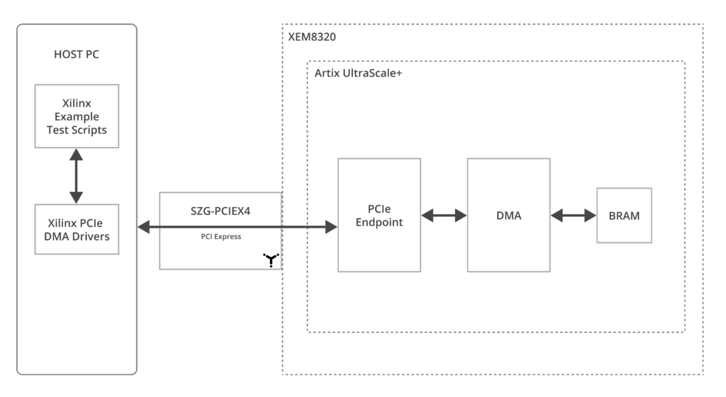
The DMA/Bridge Subsystem for PCI Express IP’s example design is generated by Vivado. The example design implements a 4KByte BRAM buffer that is read or written to via DMA. The PCIe signals travel through the Samtec cable to a SZG-PCIE4 connected to the PCIe slot on the motherboard of the HOST PC. Xilinx’s provided drivers/applications initiate the DMA transfers to and from the BRAM on the SYZYGY carrier device.
Tutorial
Create a New Vivado Project
- Open a New Vivado project.
- Select the device family for your Opal Kelly product.
- Configure the DMA/Bridge Subsystem for PCI Express IP from the IP wizard.
- Select a lane width of x4.
- Select the maximum link speed available through the GUI.
- Select Mode “Advanced”.
- Select the “GT Settings” tab.
- Select “true” for “Disable GT Channel LOC Constraint. See “Vivado IP Constraint Automation” under “Restrictions” at SZG-PCIEX4 for more information regarding why disabling the LOC constraints is necessary.
- All other settings can be kept at their default. Press “OK” to create the IP.
- Right click on the IP in the hierarchy view and select “Open IP Example Design”.
Make Board-Specific HDL Modifications
In this tutorial, you will learn how to identify which FPGA pin should be constrained to which top-level HDL port using the Pins Spreadsheet for your Opal Kelly board.
Prerequisites
- Have the example design’s constraint file available for XDC modifications.
- Have the SZG-PCIEX4 Pinout Section available.
- Have the Pins Spreadsheet accessible for your Opal Kelly board.
Steps
Step-by-Step Instruction for Identifying FPGA Pin Constraints:
- Prepare Files: Ensure you have the example design’s constraint file ready for editing. Also, keep the SZG-PCIEX4 Pinout Section available for this tutorial.
- Access Pin Lists: Go to the Pins Spreadsheet. In the “AVAILABLE PIN LISTS” section, select the product associated with your Opal Kelly board.
- Filter by Connector:
a. Click on the “DISPLAY OPTIONS” menu.
b. Choose “CONNECTOR” from the options.
c. Select the TXR4 port on your SYZYGY carrier board that you will be using with the SZG-PCIEX4. - Identify Top-Level HDL Ports: The following Top-Level HDL Ports should be connected to the corresponding Schematic Nets as specified in the SZG-PCIEX4 Pinout Section:
- sys_rst_n (Top-Level HDL Port) = PCIE_PERST_B_VIO (Schematic Net)
- sys_clk_p (Top-Level HDL Port) = PCIE_REFCLKP (Schematic Net)
- sys_clk_n (Top-Level HDL Port) = PCIE_REFCLKN (Schematic Net)
- pci_exp_txp[3:0] (Top-Level HDL Port) = PCIE_TX[3:0]P (Schematic Net)
- pci_exp_txn[3:0] (Top-Level HDL Port) = PCIE_TX[3:0]N (Schematic Net)
- pci_exp_rxp[3:0] (Top-Level HDL Port) = PCIE_RX[3:0]P (Schematic Net)
- pci_exp_rxn[3:0] (Top-Level HDL Port) = PCIE_RX[3:0]N (Schematic Net)
- Locate Schematic Net Row: In the SZG-PCIEX4 Pinout Section, find the rows associated with the Schematic Nets listed in Step 4. Take note of either the “SIGNAL NAME” or “PIN NUM” in these rows.
- Refer to Pins Spreadsheet: Return to the Pins Spreadsheet that you filtered in Step 3. Search for the “SIGNAL NAME” or “PIN NUM” you noted in Step 5.
- Match and Confirm:
a. Ensure that the “PIN NUM” from the SZG-PCIEX4 Pinout Section matches with the “PIN” column in the Pins Spreadsheet.
b. Confirm that the “SIGNAL NAME” from the SZG-PCIEX4 Pinout Section corresponds to the “DESCRIPTION” field in the Pins Spreadsheet. - Identify FPGA Pin: Once you have located the correct row in the Pins Spreadsheet, take note of the “FPGA PIN” listed for that connection.
- Update Constraint File: Use the “FPGA PIN” identified in Step 8 to set the constraints for the associated Top-Level HDL Port in the example design’s constraint file (XDC).
- Repeat for All Top-Level Ports: Repeat Steps 4 through 9 for each of the Top-Level HDL Ports specified in Step 4 to make sure all necessary ports are mapped correctly in the constraint file.
- Generate Bitstream: Once you have completed updating the XDC constraints file by adding the FPGA Pin locations for all the required Top-Level HDL Ports, save the changes and then generate the bitstream.
Example
Here is an example that demonstrates the result after following the instruction mentioned above for the XEM8320-AU25P TXR4 Port E:
set_property LOC J10 [get_ports sys_rst_n]
set_property LOC AB7 [get_ports sys_clk_p]
set_property LOC AB6 [get_ports sys_clk_n]

set_property LOC AF7 [get_ports pci_exp_txp[0]]
set_property LOC AF6 [get_ports pci_exp_txn[0]]
set_property LOC AF2 [get_ports pci_exp_rxp[0]]
set_property LOC AF1 [get_ports pci_exp_rxn[0]]

set_property LOC AE9 [get_ports pci_exp_txp[1]]
set_property LOC AE8 [get_ports pci_exp_txn[1]]
set_property LOC AE4 [get_ports pci_exp_rxp[1]]
set_property LOC AE3 [get_ports pci_exp_rxn[1]]

set_property LOC AD7 [get_ports pci_exp_txp[2]]
set_property LOC AD6 [get_ports pci_exp_txn[2]]
set_property LOC AD2 [get_ports pci_exp_rxp[2]]
set_property LOC AD1 [get_ports pci_exp_rxn[2]]

set_property LOC AC5 [get_ports pci_exp_txp[3]]
set_property LOC AC4 [get_ports pci_exp_txn[3]]
set_property LOC AB2 [get_ports pci_exp_rxp[3]]
set_property LOC AB1 [get_ports pci_exp_rxn[3]]Code language: CSS (css)
Power on Procedure
The PCIe device must be powered and available at the time the host PC enumerates the PCIe bus at power on. Follow the following procedure to configure your hardware correctly:
- Power-off all devices.
- Place the SZG-PCIEX4 into a capable PCIe slot on your host PC.
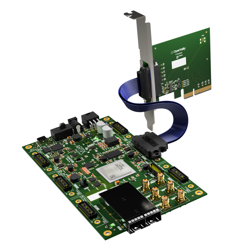
- Connect the provided Samtec cable between the SYZYGY connectors on the SZG-PCIEX4 and your SYZYGY carrier.
- Power-on your SYZYGY carrier.
- Program the PCIe DMA bitfile into your SYZYGY carrier.
- Power-on your host PC.
Confirm Enumeration
- Run
sudo lspci -vvvto see verbose information about the devices enumerated onto the PCIe bus of the host PC. The device will be enumerated under the name “Xilinx Corporation Device”.
Install Drivers
- Acquire the sources at the following Git repository: XMA
- Follow the README’s instructions for installation.
Run the Tests
- Run the following Xilinx provided tests from the XMA Git repository:
run_tests.shperform_hwcount.sh
Troubleshooting
Disclaimer
Please note that the tutorial and guidance provided for a supported SYZYGY TXR4 carrier board and the SZG-PCIEX4 are offered AS-IS, without guarantees of maintenance or official technical support from Opal Kelly. Users should be prepared to independently address any challenges that may arise, or seek assistance through our community forums.
Scope of Support
Opal Kelly’s technical support is focused on the physical connection facilitated by the SZG-PCIEX4, connecting a PCIe fin to the transceivers of the AMD FPGA on a supported SYZYGY TXR4 carrier board. We provide detailed PCB schematics for the SZG-PCIEX4, and some schematics are provided for our supported SYZYGY TXR4 carrier boards on our downloads page. If you encounter issues related to this physical setup after reviewing the schematics, we encourage you to contact us for assistance.
Beyond Our Support
For inquiries related to AMD’s implementation of their hardened PCIe IP block (PG156), including their example designs, drivers, and operating system support, please direct your questions to AMD support. These aspects fall outside the scope of Opal Kelly’s technical support.