FrontPanel SDK
Slicer
It is common for control signals to be shared across multiple modules or bussed signals to be “sliced” into separate subsets for different purposes. Use of AMD-Xilinx’s Slice IP core gets unruly as the design grows. We recommend a custom RTL Slicer to contain all your bus slicing requirements in one module.
We define a new naming convention for the sliced signals below. See Naming Convention Benefits for more information.
<Shorthand for endpoint type><Endpoint address in hexadecimal>_<bus description>_<sliced index range>_<signal description>Code language: HTML, XML (xml)Example
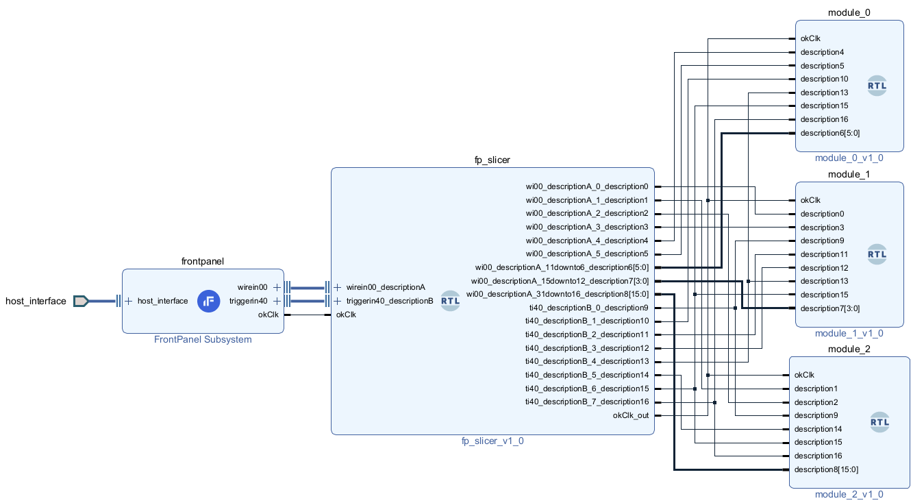
An example use case of the slicer is illustrated below in the Vivado block designer.
Here are a few examples of applying the FrontPanel API to accomplish corresponding tasks in the gateware:
SetWireInValue(0x00, 0x1 << 3, 0x1 << 3)- Bit 3 of WireIn x00 is set to
1. - The mask assures that only bit 3 is affected.
- In the block diagram, this bit is set to
module_1,description3.
- Bit 3 of WireIn x00 is set to
SetWireInValue(0x00, 0xbeef0000, 0xffff0000)- The upper word of WireIn x00 is set to
0xbeef. - The mask assures that only the upper word is affected.
- The slicer rips bits 31:16 and passes them to
module_2atdescription8[15:0]
- The upper word of WireIn x00 is set to
ActivateTriggerIn(0x40, 4)- Bit 4 of TriggerIn x40 is activated.
- The slicer rips bit 4 of the trigger bus and passes it to
module_0andmodule_1.
Slicer HDL
The code below is the input to the IPI Block Designer corresponding to the slicer described in this example.
module fp_slicer(
    (* X_INTERFACE_INFO = "opalkelly.com:interface:wirein:1.0 wirein00_descriptionA EP_DATAOUT" *)
    input  wire [31:0] wi00_ep_dataout,
    (* X_INTERFACE_INFO = "opalkelly.com:interface:triggerin:1.0 triggerin40_descriptionB EP_TRIGGER" *)
    input  wire [31:0] ti40_ep_trigger,
    (* X_INTERFACE_INFO = "opalkelly.com:interface:triggerin:1.0 triggerin40_descriptionB EP_CLK" *)
    output wire        ti40_ep_clk,

    output wire        wi00_descriptionA_0_description0,
    output wire        wi00_descriptionA_1_description1,
    output wire        wi00_descriptionA_2_description2,
    output wire        wi00_descriptionA_3_description3,
    output wire        wi00_descriptionA_4_description4,
    output wire        wi00_descriptionA_5_description5,
    output wire [5:0]  wi00_descriptionA_11downto6_description6,
    output wire [3:0]  wi00_descriptionA_15downto12_description7,
    output wire [15:0] wi00_descriptionA_31downto16_description8,

    output wire        ti40_descriptionB_0_description9,
    output wire        ti40_descriptionB_1_description10,
    output wire        ti40_descriptionB_2_description11,
    output wire        ti40_descriptionB_3_description12,
    output wire        ti40_descriptionB_4_description13,
    output wire        ti40_descriptionB_5_description14,
    output wire        ti40_descriptionB_6_description15,
    output wire        ti40_descriptionB_7_description16,

    input wire         okClk,
    output wire        okClk_out
    );

    assign wi00_descriptionA_0_description0          = wi00_ep_dataout[0];
    assign wi00_descriptionA_1_description1          = wi00_ep_dataout[1];
    assign wi00_descriptionA_2_description2          = wi00_ep_dataout[2];
    assign wi00_descriptionA_3_description3          = wi00_ep_dataout[3];
    assign wi00_descriptionA_4_description4          = wi00_ep_dataout[4];
    assign wi00_descriptionA_5_description5          = wi00_ep_dataout[5];
    assign wi00_descriptionA_11downto6_description6  = wi00_ep_dataout[11:6];
    assign wi00_descriptionA_15downto12_description7 = wi00_ep_dataout[15:12];
    assign wi00_descriptionA_31downto16_description8 = wi00_ep_dataout[31:16];

    assign ti40_descriptionB_0_description9          = ti40_ep_trigger[0];
    assign ti40_descriptionB_1_description10         = ti40_ep_trigger[1];
    assign ti40_descriptionB_2_description11         = ti40_ep_trigger[2];
    assign ti40_descriptionB_3_description12         = ti40_ep_trigger[3];
    assign ti40_descriptionB_4_description13         = ti40_ep_trigger[4];
    assign ti40_descriptionB_5_description14         = ti40_ep_trigger[5];
    assign ti40_descriptionB_6_description15         = ti40_ep_trigger[6];
    assign ti40_descriptionB_7_description16         = ti40_ep_trigger[7];

    assign ti40_ep_clk = okClk;
    assign okClk_out   = okClk;
endmodule
Code language: JavaScript (javascript)