Example: FFTScope

FFTScope is an open-source, browser-based signal generator and spectrum analyzer for Opal Kelly FPGAs. Built on FrontPanel Platform, it chains three instruments into one app: a tone-summing waveform generator that feeds the DAC, a dual-channel oscilloscope that captures the ADC input, and a spectrum analyzer that displays the FFT of that same capture.
Supported Configurations
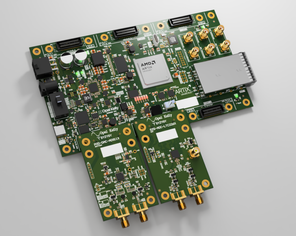
FFTScope runs on any supported host board and needs at least one of two peripherals: the SZG-DAC-AD9116 (Port A), an SZG-ADC-LTC226x variant (Port B), or both.
| Board / SYZYGY Peripheral | Sample Rate | Bit Width | Spectrum Range |
|---|---|---|---|
| XEM8320-AU25P | |||
| SZG-ADC-LTC2268 | 125 MSPS | 14-bit | 0–62.5 MHz |
| SZG-ADC-LTC2264 | 40 MSPS | 12-bit | 0–20 MHz |
| SZG-HUB1450-AU10P | |||
| SZG-ADC-LTC2268 | 80 MSPS (up to 125 MSPS)¹ | 14-bit | 0–40 MHz |
| SZG-ADC-LTC2264 | 40 MSPS | 12-bit | 0–20 MHz |
¹ Sample rate limited by what static timing analysis (STA) can close on the FPGA’s LVDS capture path in this design. The LTC2268 ADC, its LVDS routing into the FPGA, and the FPGA itself all support higher rates; reaching them requires dynamic phase alignment (DPA, per Xilinx XAPP524), which is not implemented here and is left to users to extend.
Operating Modes
The app detects which peripherals are present at startup and runs in one of three modes:
- Full — DAC on Port A and ADC on Port B. Waveform generator, oscilloscope, and spectrum analyzer are all active.
- DAC-only — DAC on Port A only. Waveform generator only.
- ADC-only — ADC on Port B only. Oscilloscope and spectrum analyzer only.
Resources
Host Boards
SYZYGY Peripherals
Links
Getting Started
You’ll need:
- A supported Board / SYZYGY Peripheral combination (see Supported Configurations)
- FrontPanel Platform 6.x installed (see the FrontPanel Platform Getting Started guide)
FFTScope.fppfrom the latest FFTScope Example Design release
To run the example design:
- Connect the SZG-DAC-AD9116 to Port A and the SZG-ADC-LTC226x to Port B on the host board. Connect a DAC output to an ADC input. Connect the board to the PC via USB, and power on.
- Install the
FFTScope.fppin the Application Launcher. - Drag the FFTScope app card onto the device card.
How To Build the Gateware
Requirements
- Vivado 2023.2 or later (Vitis Unified is bundled with Vivado; no separate Vitis install is needed)
- For XEM8320-AU25P: FrontPanel Vivado IP Core v1.0 Rev 4 or later, and XEM8320-AU25P board file v1.2 or later
- For SZG-HUB1450-AU10P: FrontPanel SDK with the BWMode3 HDL sources for SZG-HUB1450
- The latest FFTScope Example Design release source
Build steps
Each supported configuration has its own gateware folder under Gateware/<Board>/<Peripheral>/. From that folder:
- Follow the README’s one-time setup (setting
VIVADO_HOME, plus eitherFRONTPANEL_IP_REPOfor XEM8320-AU25P or a BWMode3 source copy for SZG-HUB1450-AU10P). - Run the build script (
project.baton Windows,project.shon Linux). - When Vivado opens, Generate the bitstream.
See the README in that folder for the exact commands.
How To Build the Software
Requirements
- Same development prerequisites as any FrontPanel Platform app (see the Building with NPM Create guide)
- The latest FFTScope release source
Build steps
From the Software/ folder in the release:
npm install
npm run pack
The packaged .fpp is written to Software/output/FFTScope.fpp. Pre-built bitfiles for all supported configurations ship with the repository, so you do not need to rebuild the gateware first.
Software Architecture Reference

Layers. At the top, App Shell (App.tsx) owns the device lifecycle: it opens the device, reads SYZYGY0_PRODUCT_MODEL and SYZYGY1_PRODUCT_MODEL to classify the DAC on Port A and the ADC on Port B, picks the matching bitfile from a static table, loads it, then selects AXI or Classic drivers based on the device interface type and constructs the driver trio. Below it sits the view layer: FFTScopeView composes the layout; WaveformGeneratorView, DigitizerView, TimeDomainView, SpectrumAnalyzerView, and SpectrogramView drive their respective instruments. Beneath the views, three abstract driver interfaces mirror the three gateware blocks: DigitizerDriver, SpectrumAnalyzerDriver, and WaveformGeneratorDriver. Each has two concrete implementations sitting under it: one for AXI (SZG-HUB1450-AU10P), one for Classic (XEM8320-AU25P). The drivers bottom out at the FrontPanel Platform API.
Transport seam. The three driver interfaces are where everything above becomes board-agnostic. They are implemented twice: once against IFPGADataPortAXI (native AXI on HUB1450), and once against IFPGADataPortClassic (WireIn/WireOut/TriggerIn/PipeIn/PipeOut/RegisterBridge on XEM8320). App Shell picks the matching implementation at startup. Every view above the driver layer is written against the abstract interfaces, so nothing in the UI code has to know which board it’s running on.
Gateware Architecture Reference

Data path. FFTScope runs two symmetric signal paths that meet at FrontPanel. On the capture side, the Digitizer deserializes both LVDS channels from the SZG-ADC-LTC226x on Port B, converts offset-binary samples to signed Int16, and stages them in a FIFO that FrontPanel delivers to the host as a live scope waveform. On the generate side, the host writes complex IFFT input bins into a BRAM exposed through FrontPanel, a Vitis HLS irfft core in the Waveform Generator reconstructs a time-domain waveform, and the DAC controller drives the SZG-DAC-AD9116 on Port A. Between them, the Spectrum Analyzer is a separate FFT engine that isn’t wired to the Digitizer: the host writes a waveform into it and reads back complex FFT bins (two Int32s per bin: real and imag) produced by a Vitis HLS rfft core.
Control path. Alongside the data paths, FrontPanel exposes a per-block register interface for configuration, status flags, and one-shot triggers. On SZG-HUB1450-AU10P, okHost speaks native AXI-Lite and AXI-Stream, which a SmartConnect fans out to each block. On XEM8320-AU25P, the FrontPanel Vivado IP Core exposes classic endpoints: WireIn, WireOut, and TriggerIn for registers; PipeIn and PipeOut for the Spectrum Analyzer streams; and a RegisterBridge for the Waveform Generator’s IFFT BRAM.
Release Notes
Release downloads are available on GitHub at: opalkelly-opensource/FFTScope Releases
FFTScope Example Design 1.1.0 (2026-04-20)
- Add SZG-HUB1450-AU10P host board support
- Add spectrogram mode with floor (dBFS) and contrast (gamma) adjustments
- Gateware built with Vivado 2025.2
- Bug fixes and general cleanup
FFTScope Example Design 1.0.0 (2026-04-14)
- Gateware built with Vivado 2023.2
- Initial Release