SZG-DAC-AD911X
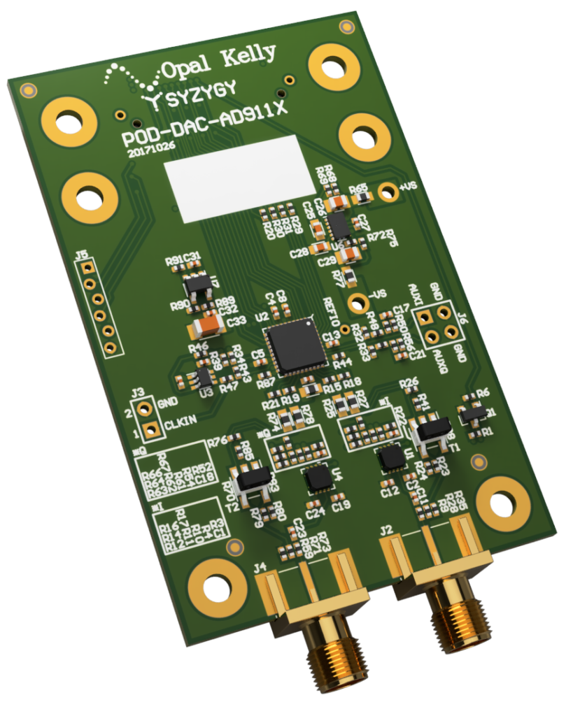
The SZG-DAC-AD911X is a dual 125 MSPS DAC module featuring the Analog Devices AD9116 TxDAC®. The module is an excellent choice for communication signal paths and general waveform synthesis applications.
In the default configuration, the SMA outputs are ac-coupled through a transformer. With some resistor changes (performed by the end user), a buffered output stage may be selected instead.
Resources
- Aligni PLM – See the Attachments tab for schematics
- SYZYGY Specification
- SYZYGY GitHub Site – Several projects that could be helpful
- SZG-DAC-AD911X Example Design
- Product Page
SYZYGY Information
Compatibility Table
| COMPATIBILITY PARAMETER | SPECIFICATION |
|---|---|
| Port type | SYZYGY Standard |
| Width | Single |
| 5V supply required | Yes |
| Nominal 5V supply current | 200mA |
| Nominal 3.3V supply current | 10mA |
| VIO supply voltage | 1.8V to 3.3V |
| Nominal VIO supply current | 20mA |
| Total number of I/O | 17 |
DNA Data
This data is stored in the SYZYGY DNA microcontroller on the SZG-DAC-AD911X peripheral.
| DNA PARAMETER | DATA |
|---|---|
| Max 5V Load | 200 mA |
| Max 3.3V Load | 10 mA |
| Max VIO Load | 20 mA |
| IS_LVDS | False |
| IS_DOUBLEWIDE | False |
| VIO Min | 1.8V |
| VIO Max | 3.3V |
Pinout
The source of the following pinout information is the SZG-DAC-AD911X schematic. This pinout follows the SYZYGY specification for STD ports.
- Column
PIN NUM (J1)lists the pin number on the SYZYGY specification’s Standard Samtec connector, this is reference designator J1 in the schematic. - Column
SIGNAL NAMElists the SYZYGY specification’s name for this pin’s connection. - Column
SCHEMATIC NETlists the net name found in the SZG-DAC-AD911X’s schematic for the connection.
| PIN NUM (J1) | SIGNAL NAME | SCHEMATIC NET | NOTE |
|---|---|---|---|
| 5 | S0 | DB0 | |
| 6 | S1 | DB1 | |
| 7 | S2 | DB2 | |
| 8 | S3 | DB3 | |
| 9 | S4 | DB4 | |
| 10 | S5 | DB5 | |
| 11 | S6 | DB6 | |
| 12 | S7 | DB7 | |
| 13 | S8 | DB8 | |
| 14 | S9 | DB9 | |
| 15 | S10 | DB10 | |
| 16 | S11 | DB11 | |
| 17 | S12 | CS_B/PWRDN | |
| 18 | S13 | SCLK/CLKMD | |
| 19 | S14 | SDIO/FORMAT | |
| 20 | S15 | OPAMP_ENABLE | Assert (1) to enable both DAC I and DAC Q outputs. Deassert (0) to place both op-amps in power-down. |
| 21 | S16 | RESET/PINMD | |
| 33 | P2C_CLKp | DCLKIO | Optional clock output (See schematics and DAC datasheet) |
| 34 | C2P_CLKp | CLKIN | Input clock to DAC through CLKIN level translator (U3) |
Design
The design of the SZG-DAC-AD911X has been heavily influenced by the evaluation board designed and produced by Analog Devices. You might find it interesting to note that we sell the SZG-DAC-AD911X for significantly less than Analog Devices sell their eval board through Digi-Key (AD9116-DPG2-EBZ-ND).
Analog Devices AD911X
From the Analog Devices datasheet:
The AD9114/AD9115/AD9116/AD9117 are pin-compatible dual, 8-/10-/12-/14-bit, low power digital-to-analog converters (DACs) that provide a sample rate of 125 MSPS. These TxDAC® converters are optimized for the transmit signal path of communication systems. All the devices share the same interface, package, and pinout, providing an upward or downward component selection path based on performance, resolution, and cost.
The AD9114/AD9115/AD9116/AD9117 offer exceptional ac and dc performance and support update rates up to 125 MSPS.
The flexible power supply operating range of 1.8 V to 3.3 V and low power dissipation of the AD9114/AD9115/AD9116/AD9117 make them well suited for portable and low power applications.
Output Stage
By default, the SZG-DAC-AD911X is configured to provide single-ended, transformer-coupled outputs to SMA connectors J2 and J4. To use the buffered output stage instead, follow the instructions in the table below. Designators are labeled on the PCB silkscreen.
| Designators | Part Size | Value | |
|---|---|---|---|
| Remove | R25, R27, R74, and R78 | 0603 | 0 Ohm |
| Place | R7, R13, R53, and R60 | 0603 | 10k Ohm |
| Remove | R28 and R79 | 0402 | 0 Ohm |
| Place | R9 and R59 | 0402 | 15 Ohm |
The bias networks for both output stages may be configured for specific applications. Refer to the additional documentation below.
Auxiliary Output
By default, the SZG-DAC-AD911X is configured to use the AD911X internal full-scale current adjust capability. In this configuration, the FSADJx/AUXx pins may be used as auxiliary DAC outputs. On the SZG-DAC-AD911X these outputs are provided on header J6. Refer to the documentation below for more information on using the auxiliary DAC outputs.
Clock Input
By default, the SZG-DAC-AD911X is configured to accept a single-ended CMOS clock over the C2P_CLKp connection from the carrier. In this configuration, the clock signal from the carrier is applied to the CLKIN and DCLKIO pins on the AD911x. If DCLKIO is configured as an output, remove R39 and place R34 — this connects DCLKIO to the P2C_CLKp pin for use on the carrier.
To apply an external clock source at J3, remove R39, R46, and R47. To apply the external clock to the DCLKIO pin, place R43. To connect the DCLKIO signal to the carrier at pin P2C_CLKp, place R34.