SZG-BRK-TXR4
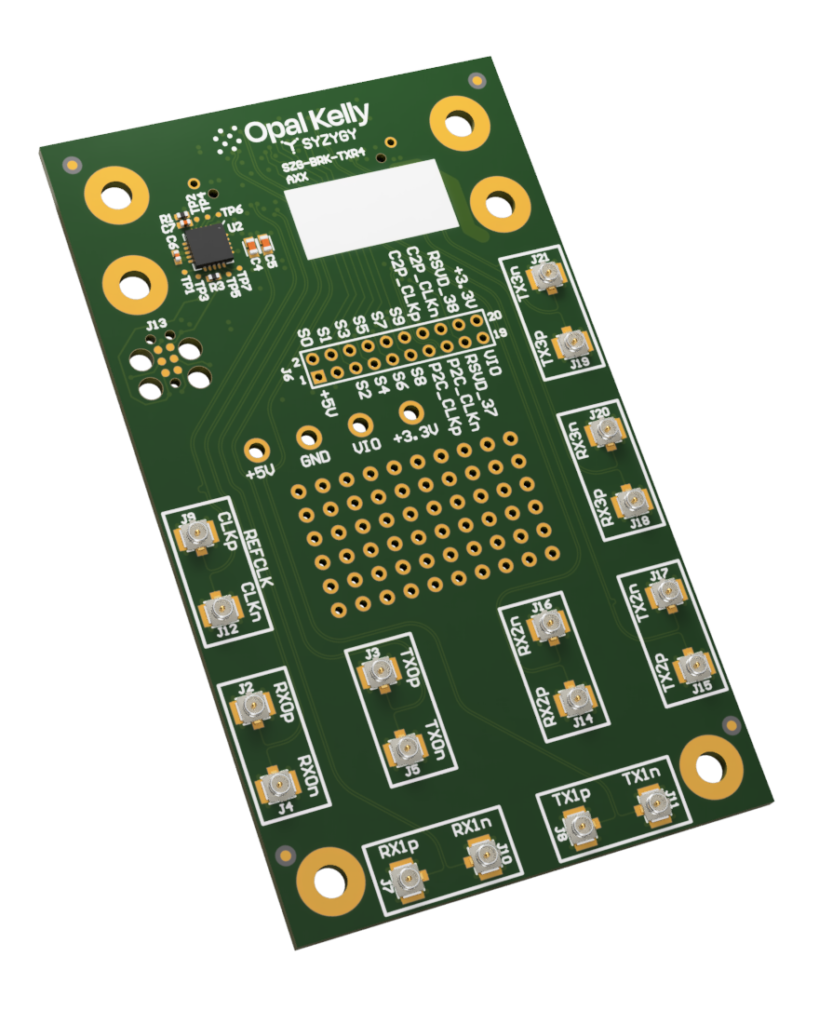
The SZG-BRK-TXR4 is a SYZYGY Transceiver (TXR4) peripheral intended to be used during early prototype development or experimentation to provide access to the high density SYZYGY ports.
Standard I/O and clocks are pinned out to a 2mm header.
Transceiver pairs are differentially routed on-board and pinned out to paired U.FL connectors at the perimeter.
Resources
- Aligni PLM – See the Attachments tab for schematics.
- SYZYGY Specification
- Product Page
I/O Voltage
The SYZYGY standard allows for a range of I/O voltage levels. Each peripheral stores it’s acceptable VIO voltage range in onboard non-volatile storage referred to as the SYZYGY DNA. The actual voltage the peripheral uses is determined by the SmartVIO calculation done by the carrier at power on. The SYZYGY carrier board will query all attached peripherals that share a specific VIO rail, compare all of their acceptable voltage ranges, and choose the lowest VIO voltage that satisfies all peripherals. If no voltage is acceptable for all peripherals, then rail stays turned off.
Breakout boards have no included peripherals to limit the I/O voltage range. Once custom hardware is added to the breakout board, a more specific I/O voltage may be desired. There are two ways to configure a specific I/O voltage with a SYZYGY breakout board.
- The best option is to change the SYZYGY DNA to a range suited for the custom hardware. This means that any SYZYGY carrier that customized breakout board is connected to will automatically compute the correct I/O voltage to use, just like with any other SYZYGY peripheral.
This provided Python tool can be used to update SYZYGY peripherals DNA (requires an MCU programmer). Edit the min and max voltage range in the SYZYGY DNA json file for the breakout board and use it with the Python tool above. - The calculated VIO solution can be overwritten using the device settings on the carrier board. You have to be more careful with this option though, as it will set the VIO voltage regardless of whether or not it is compatible with the attached peripherals.
Breakout Connections
| SYZYGY Pin | Signal | Connector | Designator |
|---|---|---|---|
| 5 | RX0P | U.FL | J2 |
| 7 | RX0N | U.FL | J4 |
| 6 | TX0P | U.FL | J3 |
| 8 | TX0N | U.FL | J5 |
| 9 | RX1P | U.FL | J7 |
| 11 | RX1N | U.FL | J10 |
| 10 | TX1P | U.FL | J8 |
| 12 | TX1N | U.FL | J11 |
| 13 | REFCLKP | U.FL | J9 [1] |
| 15 | REFCLKN | U.FL | J12 [1] |
| 29 | RX2P | U.FL | J14 |
| 31 | RX2N | U.FL | J16 |
| 30 | TX2P | U.FL | J15 |
| 32 | TX2N | U.FL | J17 |
| 25 | RX3P | U.FL | J18 |
| 27 | RX3N | U.FL | J20 |
| 26 | TX3P | U.FL | J19 |
| 28 | TX3N | U.FL | J21 |
| 14 | S0 | 2mm Header | J6-2 |
| 16 | S1 | 2mm Header | J6-4 |
| 17 | S2 | 2mm Header | J6-5 |
| 18 | S3 | 2mm Header | J6-6 |
| 19 | S4 | 2mm Header | J6-7 |
| 20 | S5 | 2mm Header | J6-8 |
| 21 | S6 | 2mm Header | J6-9 |
| 22 | S7 | 2mm Header | J6-10 |
| 23 | S8 | 2mm Header | J6-11 |
| 24 | S9 | 2mm Header | J6-12 |
| 33 | P2C_CLKP | 2mm Header | J6-13 |
| 35 | P2C_CLKN | 2mm Header | J6-15 |
| 34 | C2P_CLKP | 2mm Header | J6-14 |
| 36 | C2P_CLKN | 2mm Header | J6-16 |
| 37 | RSVD_37 | 2mm Header | J6-17 |
| 38 | RSVD_38 | 2mm Header | J6-18 |
| 2 | 5V | Test Point | TP9 and J6-1 |
| 39 | VIO | Test Point | TP10 and J6-19 |
| 40 | 3.3V | Test Point | TP8 and J6-20 |
Clock Oscillator
The SZG-BRK-TXR4 includes an onboard 125Mhz LVDS clock oscillator connected to the REFCLK input SYZYGY pins.
SYZYGY Information
Compatibility Table
| COMPATIBILITY PARAMETER | SPECIFICATION |
|---|---|
| Port type | SYZYGY Transceiver |
| Width | Single |
| 5V supply required | No |
| Nominal 5V supply current | N/A |
| Nominal 3.3V supply current | N/A |
| VIO supply voltage | 1.2V to 3.3V |
| Nominal VIO supply current | < 100mA |
| Total number of I/O | Up to 10 |
DNA Data
This data is stored in the SYZYGY DNA microcontroller on the SZG-BRK-TXR4 peripheral.
| DNA PARAMETER | DATA |
|---|---|
| Max 5V Load | 0 mA |
| Max 3.3V Load | 10 mA |
| Max VIO Load | 0 mA |
| IS_LVDS | False |
| IS_DOUBLEWIDE | False |
| VIO Min | 1.2V |
| VIO Max | 3.3V |