SZG-TST-TXR
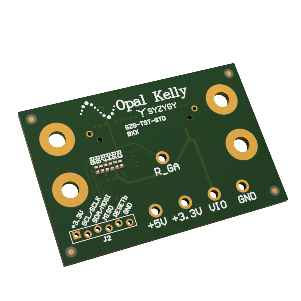
The SZG-TST-TXR is a SYZYGY Transceiver peripheral intended to be used by SYZYGY carrier developers to test continuity during development or production of their carrier. It can be used during automated testing to validate connector I/O.
Resources
- Aligni PLM – See the Attachments tab for schematics.
- SYZYGY Specification
- Product Page
SYZYGY Information
Compatibility Table
| COMPATIBILITY PARAMETER | SPECIFICATION |
|---|---|
| Port type | SYZYGY Transceiver |
| Width | Single |
| 5V supply required | Yes |
| Nominal 5V supply current | < 10mA |
| Nominal 3.3V supply current | < 10mA |
| VIO supply voltage | 1.8V |
| Nominal VIO supply current | < 100mA |
| Total number of I/O | Up to 18 |
DNA Data
This data is stored in the SYZYGY DNA microcontroller on the SZG-TST-TXR peripheral.
| DNA PARAMETER | DATA |
|---|---|
| Max 5V Load | 10 mA |
| Max 3.3V Load | 10 mA |
| Max VIO Load | 10 mA |
| IS_LVDS | False |
| IS_DOUBLEWIDE | False |
| VIO Min | 1.8V |
| VIO Max | 1.8V |
Pinout
The source of the following pinout information is the SZG-TST-TXR schematic. This pinout follows the SYZYGY specification for TXR2 ports.
- Column
PIN NUM (J1)lists the pin number on the SYZYGY specification’s Transceiver Samtec connector, this is reference designator J1 in the schematic. For connections that are looped back, both pins are listed. - Column
SIGNAL NAMElists the SYZYGY specification’s name for this pin’s connection. For connections that are looped back, both signal names are listed. - Column
SCHEMATIC NETlists the net name found in the SZG-TST-TXR’s schematic for the connection.
| PIN NUM (J1) | SIGNAL NAME | SCHEMATIC NET | NOTE |
|---|---|---|---|
| 5 <-> 6 | RX0p <-> TX0p | LOOPBACK_0P | 0.01 μF AC-coupling capacitor |
| 7 <-> 8 | RX0n <-> TX0n | LOOPBACK_0N | 0.01 μF AC-coupling capacitor |
| 9 <-> 10 | RX1p <-> TX1p | LOOPBACK_1P | 0.01 μF AC-coupling capacitor |
| 11 <-> 12 | RX1n <-> TX1n | LOOPBACK_1N | 0.01 μF AC-coupling capacitor |
| 13 | REFCLKp | REFCLKp | 125 MHz reference oscillator |
| 15 | REFCLKn | REFCLKn | 125 MHz reference oscillator |
| 17 | S2 | TEST_MODE_3 (Atmel PB0, U1 pin 11) | |
| 19 | S4 | TEST_MODE_2 (Atmel PB1, U1 pin 12) | |
| 21 | S6 | TEST_MODE_1 (Atmel PB2, U1 pin 14) | |
| 23 | S8 | TEST_MODE_0 (Atmel PA7, U1 pin 15) | |
| 14 <-> 16 | S0 <-> S1 | ||
| 18 <-> 20 | S3 <-> S5 | ||
| 22 <-> 24 | S7 <-> S9 | ||
| 25 <-> 27 | S10 <-> S12 | ||
| 26 <-> 28 | S11 <-> S13 | ||
| 29 <-> 31 | S14 <-> S16 | ||
| 30 <-> 32 | S15 <-> S17 | ||
| 33 <-> 35 | P2C_CLKp <-> P2C_CLKn | ||
| 34 <-> 36 | C2P_CLKp <-> C2P_CLKn |
Design
The SZG-TST-STD is designed to assist carrier developers perform continuity and power supply tests during development and production testing. To accomplish this, the test peripheral connects a communication path from the FPGA to the Atmel MCU for power supply tests. The remaining pins on the connector are shorted together according to the connections in the table above to allow for continuity testing.
Test Firmware
The Atmel MCU on the test peripherals contains a modified version of the normal DNA firmware. The test firmware removes the power supply sequencing options present in the standard firmware.The test firmware also uses the AVR to measure each of the power supply rails, reporting their status back to the FPGA.
Each supply rail is measured with the internal AVR ADC and checked against a pair of threshold values corresponding to the SYZYGY specified tolerance of that power supply rail. If the supply rail is within its required tolerance the AVR sets a “good” status bit for that rail. The VIO rail is assumed to be at 1.8V by the AVR firmware and the DNA for the test peripheral. A 1.8V VIO is used to maximize compatibility with current FPGA I/O supply requirements.
Supply status is communicated back to the FPGA through SYZYGY pins 5, 7, 9, and 11. The AVR continuously reads AVR pin PA7 (SYZYGY Pin 11 (S6)), then outputs the power supply state on the PB[2:0] pins according to the table below.
| +5V Supply | +3.3V Supply | VIO Supply | ||
|---|---|---|---|---|
| PA7 = 1 | Good | PB0 = 1 | PB2 = 1 | PB1 = 1 |
| Bad | PB0 = 0 | PB2 = 0 | PB1 = 0 | |
| PA7 = 0 | Good | PB0 = 0 | PB2 = 0 | PB1 = 0 |
| Bad | PB0 = 1 | PB2 = 1 | PB1 = 1 |
By toggling the PA7 pin with the FPGA it is possible to test continuity on the MCU pins while also checking the status of each power supply.