SZG-PMOD4
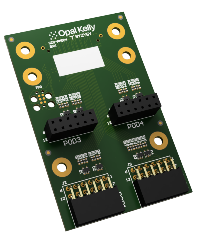
The SZG-PMOD4 is a SYZYGY Standard module that provides expansion to up to four Digilent Pmod peripherals.
Resources
- Aligni PLM – See the Attachments tab for schematics.
- SYZYGY Specification
- Product Page
SYZYGY Information
Compatibility Table
| COMPATIBILITY PARAMETER | SPECIFICATION |
|---|---|
| Port type | SYZYGY Standard |
| Width | Single |
| 5V supply required | No |
| Nominal 5V supply current | N/A |
| Nominal 3.3V supply current | < 10mA |
| VIO supply voltage | 3.3V |
| Nominal VIO supply current | Depends on Pmod peripherals |
| Total number of I/O | 32 |
| Number of differential I/O pairs | 0 |
DNA Data
This data is stored in the SYZYGY DNA microcontroller on the SZG-PMOD peripheral.
Note that the maximum VIO (configured to 3.3V) load below is an overestimate to account for the potential variability in current loads between Pmod modules.
| DNA PARAMETER | DATA |
|---|---|
| Max 5V Load | 0 mA |
| Max 3.3V Load | 0 mA |
| Max VIO Load | 1000 mA |
| IS_LVDS | False |
| IS_DOUBLEWIDE | False |
| VIO Min | 3.3V |
| VIO Max | 3.3V |
Design
The PMOD4 peripheral is a basic device that breaks out a single SYZYGY Standard port into up to 4 Digilent Pmod connectors.
Each signal is routed through a 200Ω series resistor before connecting to its corresponding SYZYGY connector pin. This is to reduce current in the case of a shorted connection to avoid damage to the FPGA I/O.
Additionally, each signal is routed through an ESD protection diode (ON Semiconductor NSQA6V8AW5T2G) on the Pmod side of the series resistor.
POD1 Connections
| PMOD I/O | SYZYGY SIGNAL | SYZYGY PIN |
|---|---|---|
| 1 | S15 | J1-20 |
| 2 | S13 | J1-18 |
| 3 | S11 | J1-16 |
| 4 | S9 | J1-14 |
| 5 | DGND | |
| 6 | +3.3VDD | |
| 7 | S14 | J1-19 |
| 8 | S12 | J1-17 |
| 9 | S10 | J1-15 |
| 10 | S8 | J1-13 |
| 11 | DGND | |
| 12 | +3.3VDD |
POD2 Connections
| PMOD I/O | SYZYGY SIGNAL | SYZYGY PIN |
|---|---|---|
| 1 | S22 | J1-27 |
| 2 | S20 | J1-25 |
| 3 | S18 | J1-23 |
| 4 | S16 | J1-21 |
| 5 | DGND | |
| 6 | +3.3VDD | |
| 7 | S23 | J1-28 |
| 8 | S21 | J1-26 |
| 9 | S19 | J1-24 |
| 10 | S17 | J1-22 |
| 11 | DGND | |
| 12 | +3.3VDD |
POD3 Connections
| PMOD I/O | SYZYGY SIGNAL | SYZYGY PIN |
|---|---|---|
| 1 | S7 | J1-12 |
| 2 | S5 | J1-10 |
| 3 | S3 | J1-8 |
| 4 | S1 | J1-6 |
| 5 | DGND | |
| 6 | +3.3VDD | |
| 7 | S6 | J1-11 |
| 8 | S4 | J1-9 |
| 9 | S2 | J1-7 |
| 10 | S0 | J1-5 |
| 11 | DGND | |
| 12 | +3.3VDD |
POD4 Connections
| PMOD I/O | SYZYGY SIGNAL | SYZYGY PIN |
|---|---|---|
| 1 | C2P_CLKn | J1-36 |
| 2 | C2P_CLKp | J1-34 |
| 3 | S27 | J1-32 |
| 4 | S25 | J1-30 |
| 5 | DGND | |
| 6 | +3.3VDD | |
| 7 | P2C_CLKn | J1-35 |
| 8 | P2C_CLKp | J1-33 |
| 9 | S26 | J1-31 |
| 10 | S24 | J1-29 |
| 11 | DGND | |
| 12 | +3.3VDD |
Product Lifecycle
PCB Revision History
| Revision | DETAIL |
|---|---|
| 20170719 | First production PCB. |
| BXX | Use VIO (at 3.3V) as PMOD power instead of SYZYGY 3.3V |
Known Issues
VIO Back Powering
SZG-PMOD4 boards with PCB date code 20170719 are designed such that the 3.3V rail powers all Pmod peripherals connected to the SZG-PMOD4. It is possible for Pmod peripherals to back power the VIO rail through FPGA I/O internal clamp diodes under the following conditions:
- +3.3V power is enabled while +VIO is disabled. The SYZYGY specification calls for +3.3V to turn on first. The carrier implementation and peripheral configuration determines how long this condition lasts. It could be short (10’s of milliseconds) or it could be indefinite (if VIO is never enabled).
- The peripheral drives (applies) a voltage onto the I/O pins.
The scope of the issue depends on the specific carrier and peripherals in an application. Damage can occur to the FPGA is the back current applied to the pin exceeds 10mA. On the Opal Kelly XEM7320, there are no other significant power users attached to the VIO and no VIO is shared among peripherals. Therefore, no significant current would pass through the clamp diodes. On the Opal Kelly Brain-1, a second peripheral on the same VIO bank could draw current and force this current through the clamp diodes. Other carrier designs may also experience damage if their VIO power supply design is capable of sinking current prior to the VIO rail powering on.
Current Rev BXX boards use VIO as the PMOD power rail, automatically assigning it to 3.3V via SmartVIO. This prevents any back powering issues.
If you have any questions or comments, please feel free to reach out to Opal Kelly Support.