SZG-DISPLAYPORT
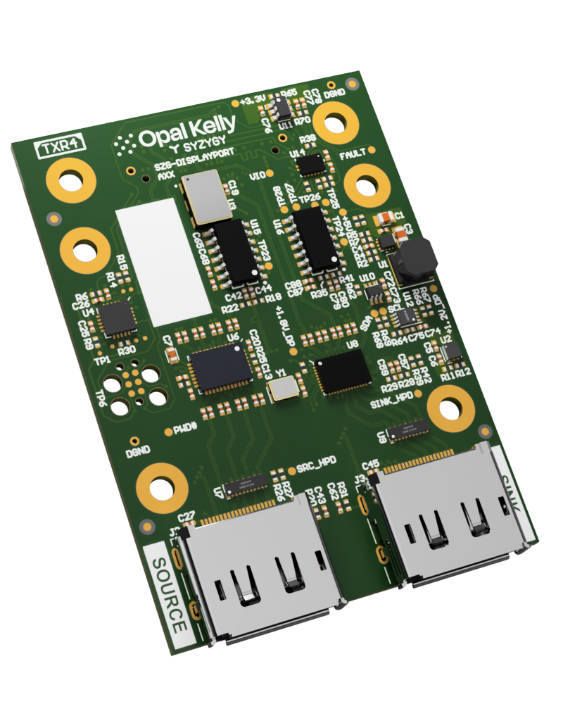
The SZG-DISPLAYPORT is a dual DisplayPort 1.4 capable module with one source and one sink port. It features a Texas Instruments SN65DP141RLJ re-driver on the source port, and a Kinetic Technologies MCDP6000C1 re-timer on the sink port. This module is an excellent choice for development of DisplayPort input, output, or performing real-time analysis, processing, or editing of pass-through video.
Resources
- Aligni PLM – See the Attachments tab for schematics
- SYZYGY Specification
- SYZYGY GitHub Site – Several projects that could be helpful
- DisplayPort Example Design
- Product Page
Design
Transceivers
The DisplayPort source port uses all 4 of the SYZYGY TXR4 ports transceiver TX lanes, while the sink port uses all 4 of the RX lanes. The source and sink ports utilizes a redriver and a retimer, respectively.
Redriver/Retimer
| Part | Manufacturer | Part Number | I2C Address |
|---|---|---|---|
| Source port Redriver | Texas Instruments | SN65DP141RLJ | 0000 010x |
| Sink port Retimer | Kinetic Technologies | MCDP6000C1 | 0010 100x |
Source Port Connections
| SYZYGY Port Pin | Signal Name | Type | Description |
|---|---|---|---|
S2 | DP_SRC_HPD | Input | Hot Plug Detect |
S4 | DP_SRC_AUX_TX_EN | Output | AUX channel TX enable |
S6 | DP_SRC_AUX_RX | Input | AUX channel Single-Ended RX |
S8 | DP_SRC_AUX_TX | Output | AUX channel Single-Ended TX |
S0 | DP_SDA | I/O | Redriver I2C Bus |
S1 | DP_SCL | I/O | Redriver I2C Bus |
TX0p | DP_TX0_P | Output | Source Lane 0 P |
TX0n | DP_TX0_N | Output | Source Lane 0 N |
TX1p | DP_TX1_P | Output | Source Lane 1 P |
TX1n | DP_TX1_N | Output | Source Lane 1 N |
TX2p | DP_TX2_P | Output | Source Lane 2 P |
TX2n | DP_TX2_N | Output | Source Lane 2 N |
TX3p | DP_TX3_P | Output | Source Lane 3 P |
TX3n | DP_TX3_N | Output | Source Lane 3 N |
Sink Port Connections
| SYZYGY PORT PIN | SIGNAL NAME | Type | DESCRIPTION |
|---|---|---|---|
S3 | DP_SINK_HPD | Output | Hot Plug Detect |
S5 | DP_SINK_AUX_TX_EN | Output | AUX channel TX enable |
S7 | DP_SINK_AUX_RX | Input | AUX channel Single-Ended RX |
S9 | DP_SINK_AUX_TX | Output | AUX channel Single-Ended TX |
S0 | DP_SDA | I/O | Redriver I2C Bus |
S1 | DP_SCL | I/O | Redriver I2C Bus |
RX0p | DP_RX0_P | Input | Sink Lane 0 P |
RX0n | DP_RX0_N | Input | Sink Lane 0 N |
RX1p | DP_RX1_P | Input | Sink Lane 1 P |
RX1n | DP_RX1_N | Input | Sink Lane 1 N |
RX2p | DP_RX2_P | Input | Sink Lane 2 P |
RX2n | DP_RX2_N | Input | Sink Lane 2 N |
RX3p | DP_RX3_P | Input | Sink Lane 3 P |
RX3n | DP_RX3_N | Input | Sink Lane 3 N |
Connectors
The module includes two full size DisplayPort connectors. Providing both a DisplayPort source and sink.
Refclock
The onboard 270 MHz reference clock provides the clock source required for DisplayPort 1.4 operation.
See Xilinx document PG230 table 75 and 76 for refclock requirements at different line rates.
SYZYGY Information
Compatibility Table
| COMPATIBILITY PARAMETER | SPECIFICATION |
|---|---|
| Port type | SYZYGY Transceiver TXR4 |
| Width | Single |
| 5V supply required | Yes |
| Nominal 5V supply current | 150 mA |
| Nominal 3.3V supply current | 500 mA |
| VIO supply voltage | 1.2V – 3.3V |
| Nominal VIO supply current | 10 mA |
| Total number of I/O | 10 |
| Number of differential I/O pairs | 0 |
DNA Data
| DNA PARAMETER | DATA |
|---|---|
| Max 5V Load | 150 mA |
| Max 3.3V Load | 500 mA |
| Max VIO Load | 10 mA |
| IS_LVDS | False |
| IS_DOUBLEWIDE | False |
| IS_TXR4 | True |
| VIO Range(s) | [1.2,3.3] |
Pinout
The source of the following pinout information is the SZG-DISPLAYPORT schematic. This pinout follows the SYZYGY specification for TXR4 ports.
- Column PIN NUM (J1) lists the pin number on the SYZYGY specification’s Standard Samtec connector, this is reference designator J1 in the schematic.
- Column SIGNAL NAME lists the SYZYGY specification’s name for this pin’s connection.
- Column SCHEMATIC NET lists the net name found in the SZG-DISPLAYPORT’s schematic for the connection.
| PIN NUM (J1) | SIGNAL NAME | SCHEMATIC NET |
|---|---|---|
| 5 | RX0p | DP_RX0_P |
| 7 | RX0n | DP_RX0_N |
| 6 | TX0p | DP_TX0_P |
| 8 | TX0n | DP_TX0_N |
| 9 | RX1p | DP_RX1_P |
| 11 | RX1n | DP_RX1_N |
| 10 | TX1p | DP_TX1_P |
| 12 | TX1n | DP_TX1_N |
| 13 | REFCLKp | REFCLK_C_P |
| 15 | REFCLKn | REFCLK_C_N |
| 14 | S0 | DP_SDA_VIO |
| 16 | S1 | DP_SCL_VIO |
| 17 | S2 | DP_SRC_HPD_VIO |
| 19 | S4 | DP_SRC_AUX_TX_EN_VIO |
| 18 | S3 | DP_SINK_HPD_VIO |
| 20 | S5 | DP_SINK_AUX_TX_EN_VIO |
| 21 | S6 | DP_SRC_AUX_RX_VIO |
| 23 | S8 | DP_SRC_AUX_TX_VIO |
| 22 | S7 | DP_SINK_AUX_RX_VIO |
| 24 | S9 | DP_SINK_AUX_TX_VIO |
| 25 | RX3p | DP_RX3_P |
| 27 | RX3n | DP_RX3_N |
| 26 | TX3p | DP_TX3_P |
| 28 | TX3n | DP_TX3_N |
| 29 | RX2p | DP_RX2_P |
| 31 | RX2n | DP_RX2_N |
| 30 | TX2p | DP_TX2_P |
| 32 | TX2n | DP_TX2_N |