SZG-MIPI-8320
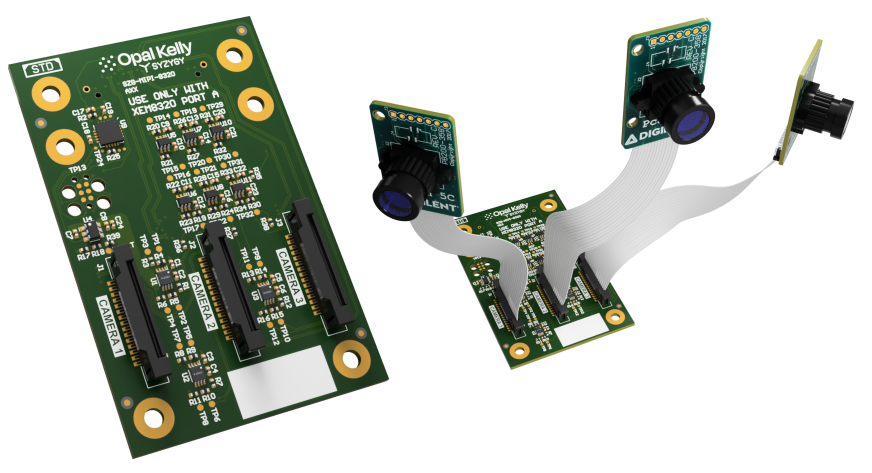
The SZG-MIPI-8320 is a breakout board allowing connection of up to three 2-lane MIPI CSI-2 cameras to port A on the XEM8320-AU25P development platform. The IO requirements for this peripheral makes it only compatible with Port A.
Resources
- Aligni PLM – See the Attachments tab for schematics.
- Camera Reference Design – Full-featured image capture gateware and software example.
- SYZYGY Specification
- SYZYGY GitHub Site – Several projects that could be helpful.
- Product Page
Design
XEM8320 Port A Only
HP banks 66 and 67 on the XEM8320-AU25P have their VRP pin connected to ground through a 240 ohm resistor, this is a requirement to use the MIPI_DPHY_DCI IOSTANDARD. Careful IO planning was done with port A’s connection to bank 66 as well as SZG-MIPI-8320’s connections to port A to ensure that three 2-lane MIPI cameras could be used on this port. IO requirements from PG202 and PG232 were followed as well as ensuring all MIPI lanes are placed onto differential pairs of port A, which are length matched ≤10 mils as per Port A’s SYZYGY compatibility table.
IO Planning
- The CLOCK for MIPI must use a
QBCorDBCpair - A
DBCclock can only be used by data pairs in the same byte group of the bank - A
QBCclock can be used by any data pair on the same bank - Highly recommended that the MIPI clock and data pairs be in numerical order, i.e. N0 to N5 of the byte group for one camera. Otherwise additional pin resourced must be used to propagate the signal.
These rules were followed and the following connections established for the SZG-MIPI-8320 paired with port A. Only the P side of the pair is listed. The following information is formatted to directly correspond with the configuration presentation used within Xilinx’s MIPI IPs. You may input the following information directly into the IP wizard to configure the cameras of your choosing.
| Name | Pin Loc | Pin Name |
|---|---|---|
| Clock Lane | L18 | IO_L1P_T0L_N0_DBC_66 |
| Data Lane0 | M20 | IO_L2P_T0L_N2_66 |
| Data Lane1 | J19 | IO_L3P_T0L_N4_AD15P_66 |
| Name | Pin Loc | Pin Name |
|---|---|---|
| Clock Lane | L22 | IO_L7P_T1L_N0_QBC_AD13P_66 |
| Data Lane0 | M25 | IO_L8P_T1L_N2_AD5P_66 |
| Data Lane1 | K25 | IO_L9P_T1L_N4_AD12P_66 |
| Name | Pin Loc | Pin Name |
|---|---|---|
| Clock Lane | L24 | IO_L10P_T1U_N6_QBC_AD4P_66 |
| Data Lane0 | K22 | IO_L11P_T1U_N8_GC_66 |
| Data Lane1 | J23 | IO_L12P_T1U_N10_GC_66 |
Connector
Three 15 pin FPC connectors that follow the CSI-2 standard are used on the SZG-MIPI-8320. 2-lane MIPI cameras will typically use the 15 pin connector as it will fully populate with 2-lanes. This is in contrast to 22 pin connectors typically seen in 4-lane MIPI cameras. We list camera options below in “Camera Options” that are 2-lane using the 15 pin connector.
GPIO
Two GPIO are available per camera. GPIO0 (Connector pin 11) is used as a power enable. GPIO1 (Connector pin 12) is multi-use, determined by the camera used.
Because GPIO1 is multi-use, it could either be an input or an output. We provide a direction pin (GPIO1_DIR) connected to the level translators for the GPIO1s to control their direction. Because of the limited IO on port A, GPIO1_DIR controls the direction for all three camera’s GPIO1.
Camera Options
The following is a list of CSI-2 compatible camera modules. They all follow the standard 15 pin FPC connector pinout, but have a variety of uses for the extra GPIO1 pin.
Of the following cameras, we have only tested the SZG-MIPI-8320 with the Digilent PCam 5C. We will be releasing sources for a single and three Pcam port of the Camera Reference Design in the next release.
| Model Number | Manufacturer | Sensor | Resolution | Power Usage | Power Enable Setup (GPIO0) | GPIO1 | Features |
|---|---|---|---|---|---|---|---|
| Pi Camera V1.3 | Raspberry Pi | OmniVision OV5647 | 5MP 2592 × 1944 | 200-250mA | LED Indicator | ||
| Pi Camera V2.1 | Raspberry Pi | Sony IMX219 | 8MP 3280 × 2464 | 200-250mA | LDO Enable | NC | |
| Pi HQ Camera | Raspberry Pi | Sony IMX477 | 12.3MP 4056 x 3040 | 200-250mA | Regulator Enable | Sensor IC GPO pin | |
| PCam 5C | Digilent | OV5640-A71A | 5MP | 200mA | LDO Enable | Optional CLK input (0R No Place Jumper) | M12 Lens |
| Pivariety 16MP | Arducam | IMX298 | 16MP 4656 × 3496 | Unknown | Unknown | Unknown | Programmable focus control |
| Pivariety 21MP | Arducam | IMX230 | 21MP 5344 × 4012 | Unknown | Unknown | Unknown | Programmable focus control |
Vivado Board File
A companion card board file is available for this SYZYGY peripheral. This companion card board file is only compatible with Port A on the XEM8320-AU25P’s board file.
Version 1.0 is currently provides the following components:
- Two MIPI lane camera module (three total for camera 1-3)
- I2C camera control interfaces (three total for camera 1-3)
- Camera reset (three total for camera 1-3)
How-To Install
Follow the appropriate installation instructions at Vivado Board Files.
Notes
- SZG-MIPI-8320 is a Port A only peripheral. You should only add this Companion Card to Port A. Port A’s connection to the I/O bank is able to support 3 two lane MIPI cameras. The other SZG-STD HP bank ports (B and C) do not have this guarantee.
- When the Camera components are placed into the IPI, or connected through the IP Wizard, they will instantiate the MIPI CSI-2 RX Subsystem IP and apply preset configurations for the Diligent Pcam operating at 1080p, 30FPS (420Mbps/Lane). This is the same configuration used in the SZG-MIPI-8320 Camera Reference Design sources. These configurations may be changed as desired.
- SZG-MIPI-8320 will set the VIO to 1.2V to support the MIPI_DPHY_DCI IOSTANDARD. As a result, it is known exactly which voltage will power this bank. When using this Companion Card the IOSTANDARD for the pins connected to this peripheral are set to MIPI_DPHY_DCI for the MIPI connections and LVCMOS12 for the GPIO connections. It is not necessary to constrain these at the top level or through the GUI.
SYZYGY Information
Compatibility Table
| COMPATIBILITY PARAMETER | SPECIFICATION |
|---|---|
| Port type | SYZYGY Standard |
| Width | Single |
| 5V supply required | No |
| Nominal 5V supply current | N/A |
| Nominal 3.3V supply current | 750mA |
| VIO supply voltage | 1.2V |
| Nominal VIO supply current | N/A |
| Total number of I/O | 13 |
| Number of differential I/O pairs | 18 |
DNA Data
| DNA PARAMETER | DATA |
|---|---|
| Max 5V Load | 0mA |
| Max 3.3V Load | 1000mA |
| Max VIO Load | 10mA |
| IS_LVDS | False |
| IS_DOUBLEWIDE | False |
| IS_TXR4 | False |
| VIO Range(s) | [1.2,1.2] |
Pinout
The source of the following pinout information is the SZG-MIPI-8320 schematic. This pinout follows the SYZYGY specification for STD ports.
- Column
PIN NUM (J4)lists the pin number on the SYZYGY specification’s Standard Samtec connector, this is reference designator J4 in the schematic. - Column
SIGNAL NAMElists the SYZYGY specification’s name for this pin’s connection. - Column
SCHEMATIC NETlists the net name found in the SZG-MIPI-8320’s schematic for the connection.
| PIN NUM (J4) | SIGNAL NAME | SCHEMATIC NET |
|---|---|---|
| 5 | D0P | CAM1_CLK_P |
| 7 | D0N | CAM1_CLK_N |
| 9 | D2P | CAM1_LANE0_P |
| 11 | D2N | CAM1_LANE0_N |
| 13 | D4P | CAM1_LANE1_P |
| 15 | D4N | CAM1_LANE1_N |
| 22 | S17 | CAM1_SCL_VIO |
| 24 | S19 | CAM1_SDA_VIO |
| 21 | S16 | CAM1_GPIO0_VIO |
| 23 | S18 | CAM1_GPIO1_VIO |
| 17 | D6P | CAM2_CLK_P |
| 19 | D6N | CAM2_CLK_N |
| 6 | D1P | CAM2_LANE0_P |
| 8 | D1N | CAM2_LANE0_N |
| 14 | D5P | CAM2_LANE1_P |
| 16 | D5N | CAM2_LANE1_N |
| 26 | S21 | CAM2_SCL_VIO |
| 28 | S23 | CAM2_SDA_VIO |
| 25 | S20 | CAM2_GPIO0_VIO |
| 27 | S22 | CAM2_GPIO1_VIO |
| 10 | D3P | CAM3_CLK_P |
| 12 | D3N | CAM3_CLK_N |
| 18 | D7P | CAM3_LANE0_P |
| 20 | D7N | CAM3_LANE0_N |
| 33 | P2C_CLKp | CAM3_LANE1_P |
| 35 | P2C_CLKn | CAM3_LANE1_N |
| 30 | S25 | CAM3_SCL_VIO |
| 32 | S27 | CAM3_SDA_VIO |
| 29 | S24 | CAM3_GPIO0_VIO |
| 31 | S26 | CAM3_GPIO1_VIO |
| 34 | C2P_CLKp | GPIO1_DIR |