SYZYGY Ports
The XEM8320 provides 4x SYZYGY Standard ports and 2x SYZYGY Transceiver (TXR4) ports to connect a variety of SYZYGY peripherals.
Documentation and Reference Materials
| XEM8320 Pins Reference | The interactive Pins reference for the device provides detailed pinout information as well as automated constraint file generation. Export functionality is provided to PDF, CSV. Constraint files are provided in XDC format for use in Vivado. |
| SYZYGY Specification | Further information and specification standard for SYZYGY ports. |
| SYZYGY GitHub | Open source SYZYGY tools and peripheral PCB template design files. |
| SYZYGY Design Guide | Design guide for connecting custom hardware to SYZYGY ports, or creating SYZYGY peripherals. |
Port Summary
| PORT | SYZYGY TYPE | SMARTVIO GROUP | VIO RANGE | REFDES | I/O Count | BANK TYPE | Bank |
|---|---|---|---|---|---|---|---|
| PORT A – SYZYGY0 | STD | 1 | 1.0 – 1.8V | J5 | 28/28 | HP | I/O 66 |
| PORT B – SYZYGY1 | STD | 1 | 1.0 – 1.8V | J6 | 28/28 | HP | I/O 66 & 67 |
| PORT C – SYZYGY2 | STD | 1 | 1.0 – 1.8V | J7 | 28/28 | HP | I/O 67 |
| PORT D – SYZYGY3 | STD | 2 | 1.2 – 3.3V | J8 | 28/28 | HD | I/O 84 & 87 |
| PORT E – SYZYGY4 | TXR4 | 3 | 1.2 – 3.3V | J9 | 10/10 | HD + GTY | GTY 224 (REFCLK 0) I/O 86 |
| PORT F – SYZYGY5 | TXR4 | 3 | 1.2 – 3.3V | J10 | 8/10 | HD + GTY | GTY 225 (REFCLK 0) I/O 86 |
Port Power
Three software controlled dc-dc regulators power the three SYZYGY SmartVIO groups as assigned above. The behavior of these power supplies is determined by the XEM8320_SMARTVIO_MODE parameter in Device Settings and associated settings. The modes function as described below.
Note that, for modes that require a SmartVIO solution, if any peripheral provides non-compliant DNA, a SmartVIO solution cannot be reached for all groups.
- SmartVIO only – SmartVIO is tested collectively so all present SmartVIO peripherals must result in a collective validation for any of the outputs to be enabled.
- SmartVIO hybrid mode – Each group is individually tested for SYZYGY peripherals. Within each group, if a SYZYGY peripheral is present (via detection of compliant DNA data) on any of the ports within that group, the SmartVIO solution is used to determine the voltage setting. If no SYZYGY peripherals are detected within the group, then the corresponding Device Setting (e.g.
XEM8320_VIO1_VOLTAGE) is used. - Device Settings only – SmartVIO settings from the peripherals are ignored, only the device settings are used. Also note that, in this mode, SYZYGY peripheral discovery is not performed so the corresponding device settings that identify each peripheral are not populated.
SmartVIO Operation
The SmartVIO solution for each group is determined by the voltage range(s) supported by the corresponding FPGA I/O banks and the voltage range(s) supported by the peripherals, as reported in their respective SYZYGY DNA. The process is as follows:
- The SmartVIO controller (XEM8320) queries all detected peripherals for their SYZYGY DNA.
- The controller attempts to determine the lowest voltage that will satisfy all attached peripherals and FPGA ranges.
- If a solution is not found, the group voltage remains disabled to protect any incompatible devices on the group.
- If a solution is found, the group voltage is set to the voltage and enabled.
Peripherals that use LVDS may have a fixed or limited voltage range depending on the carrier. LVDS usage is stored as a flag in the peripherals SYZYGY DNA. Commonly this will limit the SmartVIO solution to 1.8V or 2.5V depending on the I/O bank type connected to the SYZYGY port (as with the XEM8320), but other voltages may be set depending on the specific FPGA requirements.
Port Current Supply
The SYZYGY power rails current output is limited by the regulator used on the carrier as well as the current carrying capacity of the SYZYGY connector. The on-board regulator limits are listed on each carriers SYZYGY Compatibility Table (see below) which shows the total current output maximum for all of the ports combined. Each individual port is limited to 2A output for each of the 3 SZYGY power rails (3.3V, 5V, and VIO) by the current carrying capacity of the SYZYGY connector.
+5V and +3.3V Supplies
The SYZYGY +5V and +3.3V supplies are enabled during the firmware boot process. The switching regulator used for these supplies operates in a “light load mode” for efficiency when the load is relatively small. This light load operation can result in higher supply ripple, a common behavior among such supplies. This is normal, but may be higher than some applications desire. SYZYGY peripherals that are sensitive to high ripple should use additional power regulation on these supply rails.
The +5V and +3.3V regulators (Texas Instruments TPS54429E) include a light-load mode which increases regulator efficiency at the expense of output voltage ripple. In normal mode, the switching frequency is 700 kHz. In light-load mode, the effective switching frequency is reduced substantially (<10 kHz in some cases). The transition point between normal operation and light-load operation is dependent on the input supply voltage to the XEM8320, but typically occurs between 0.5 and 1.0 A output current. Output voltage ripple in light-load mode can be in the range of 50-100 mVpp.
VRP Pins
SYZYGY ports A through C are connected to HP banks 66 and 67. These banks have their VRP pin connected to ground through a 240 ohm resistor. This is a requirement to use various high performance IOSTANDARDs.
Using these high performance IOSTANDARDs that utilize the VRP pins typically require strict pin placement to data and clock designated pins within the same IO byte group of a bank. Using the Pins Spreadsheet paired with the AU25P FFVB676 Package Device Pinout file, you’ll be able to make a correlation between the SYZYGY connector pin and the associated AMD full pin name, i.e., IO_L7N_T1L_N1_QBC_AD13N_66. Definitions of the various identifiers within the full name are at UG575.
Our provided schematics for the XEM8320-AU25P visualizes the AMD full pin name and the connection to the associated SYZYGY connector pin. Connections are listed in byte group ascending order which will help aid in verifying the strict pin requirements to data and clock designated pins.
The SZG-MIPI-8320 is an example peripheral that utilizes these VRP pins to use the MIPI_DPHY_DCI IOSTANDARD. The SZG-MIPI-8320’s documentation discusses this in more detail.
Considerations for Differential Signals
The XEM8320 PCB layout and routing has been designed with several applications in mind, including applications requiring the use of differential (LVDS) pairs. Please refer to the Artix UltraScale+ datasheet for details on using differential I/O standards with the Artix UltraScale+ FPGA.
Impedance and Length Matching
Single-ended fabric I/O are routed to the SYZYGY ports with 50Ω characteristic impedance. Differential fabric I/O and transceiver signals are routed to the SYZYGY ports as pairs with 100Ω differential impedance. Pin/package delay information may be obtained from the AMD design tools. The additional notes below also apply.
- Opal Kelly has matched fabric I/O routing to each SYZYGY port within 100 mil (2.54 mm). This matching includes the pin/package delays of the Artix UltraScale+.
- The length matching numbers in the compatibility tables below represent routed PCB lengths only and do not include the pin/package delays.
- Individual PCB routing lengths for all SYZYGY I/O (including transceivers) is available on the XEM8320 Pins Reference page. The lengths published there represent routed PCB lengths only and do not include the pin/package delays.
FPGA Differential I/O Standards
The different I/O banks on the Artix UltraScale+ have different features and specific requirements needed to use differential I/O standards.
HP banks support LVDS inputs and outputs. The bank VCCO must be set to 1.8V to use LVDS outputs. This also allows the use of the available internal termination on LVDS inputs.
HD banks only support LVDS inputs, and only with external termination. The XEM8320 provides optional external termination resistor positions under the FPGA. As such termination would interfere with the I/O being used as single ended connections, these termination resistors are not populated by default. See the XEM8320 schematics to find the termination resistor designator for each HD bank differential pair. The resistor designators are marked on the PCB silkscreen. 100 Ohm resistors can be placed as external termination for each pair.
The bank type associated with each SYZYGY port is listed in the Port Summary above.
Please see LVDS Interface Checklist for more information. Also see DS931 for information regarding the LVDS DC Specifications on the Artix UltraScale+. For more information on the differential I/O standard limitations of HD banks see the “High Density I/O Resources” section of UG571.
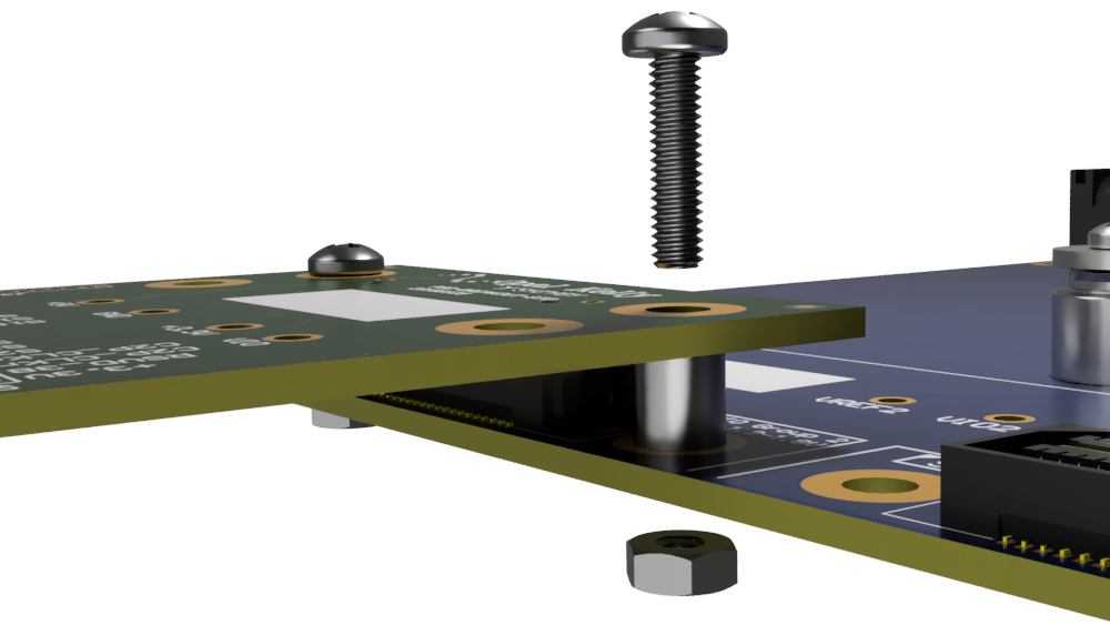
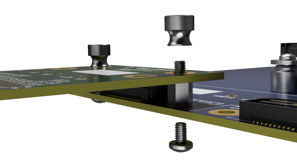
Peripheral Mounting
SYZYGY peripherals can be mechanically connected together using the carrier and peripheral mounting holes. Below are some suggested mounting hardware options. The Standard Hardware mounting kit is available from the accessories section of our store.
| Part | Supplier | PART NUMBER | QUANTITY per port |
|---|---|---|---|
| 5mm Unthreaded Standoff | McMaster-Carr | 94669A098 | 2 |
| Pan Head Phillips 10mm Bolt | McMaster-Carr | 92000A106 | 2 |
| Hex Nut | McMaster-Carr | 91828A113 | 2 |
| Part | Supplier | PART NUMBER | QUANTITY per port |
|---|---|---|---|
| Male-to-Female 5mm Standoff | McMaster-Carr | 93655A001 | 2 |
| Pan Head Phillips 4mm Bolt | McMaster-Carr | 92000A102 | 2 |
| Thumb Nut | McMaster-Carr | 96445A320 | 2 |
SYZYGY Compatibility Table
Rev BXX
|
PARAMETER |
PORT A |
PORT B |
PORT C |
PORT D |
PORT E |
PORT F |
|---|---|---|---|---|---|---|
|
Total 5V Supply Current |
4.5 A |
|||||
|
Total 3.3V Supply Current |
4.5 A |
|||||
|
Port Groups |
Group 1: A, B, C |
Group 2: D |
Group 3: E, F |
|||
|
Port Type |
Standard |
Standard |
Standard |
Standard [1, 2] |
Transceiver (TXR4) [2] |
Transceiver (TXR4) [2] |
|
Bank Type |
HP |
HP |
HP |
HD |
GTY + HD |
GTY + HD |
|
VIO Supply Voltage Range |
1.0 – 1.8 V |
1.2 – 3.3 V |
1.2 – 3.3 V |
|||
|
Total VIO Supply Current |
1 A |
1 A |
1 A |
|||
|
Port Spacing |
Double-Wide Spacing |
Single-Wide |
Double-Wide Spacing |
|||
|
I/O per Port |
28 total |
28 total |
28 total |
28 total |
10 total |
6 total |
|
Length Matching |
3602 – 3943 mils DP: 5 mils max |
1994 – 2325 mils DP: 5 mils max |
2963 – 3236 mils DP: 5 mils max |
3791 – 4176 mils |
Single-Ended: 2731 – 2853 mils Transceivers: 1445 – 2282 mils |
Single-Ended: 3130 – 3310 mils Transceivers: 2091 – 2928 mils |
- The I/O on this port do not support differential standards because of limitations on HD banks.
- The C2P and P2C clock pins on these ports do not support differential standards because of limitations on HD banks.