JTAG and SYSMON
JTAG USB (Rev CXX and Later)
On XEM8320 rev CXX and later (purchased on or after 2023 July 28 or so), an on board JTAG adapter is included. A vertical-launch USB Type-C connector provides JTAG access to the FPGA and only requires a standard USBC cable for connection to the host computer. This interface is supported by the vendor tools for JTAG communication (i.e. Vivado Integrated Logic Analyzer).
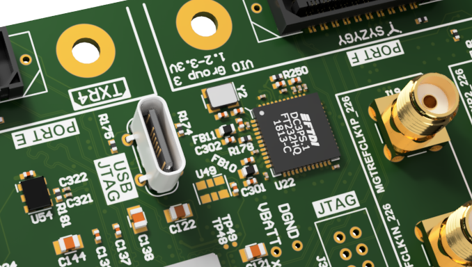
The direct access JTAG header (see the BXX header information below) is still available on revision CXX boards, but the header connector is not placed by default. The connector (Molex 87831-1420 or compatible) would need to be placed to use the direct JTAG connections.
JTAG Header (Rev BXX and Earlier)
The JTAG connections on the FPGA are wired directly to a dedicated 2mm header (J3) facilitate FPGA configuration and ChipScope usage using a JTAG cable. The JTAG interface presented is a 1.8V interface corresponding to the FPGA JTAG I/O voltage. The TMS, TCK and TDI signals are pulled to 1.8V via 4.75k resistors.
| CONNECTOR PIN | JTAG SIGNAL | CONNECTOR PIN | JTAG SIGNAL | FPGA Pin |
|---|---|---|---|---|
| 1 | GND | 2 | +1.8V (Vref) | |
| 3 | GND | 4 | JTAG_TMS | AB10 |
| 5 | GND | 6 | JTAG_TCK | AE12 |
| 7 | GND | 8 | JTAG_TDO | Y10 |
| 9 | GND | 10 | JTAG_TDI | AB12 |
| 11 | GND | 12 | NC | |
| 13 | GND | 14 | NC |
JTAG Header Cables
A vendor-supported JTAG cable is required to interface with the JTAG header connector and provide tool access to JTAG. The JTAG cables listed below are available with connectors compatible with the connector on the XEM8320.
| FPGA COMPATIBILITY | MANUFACTURER | CABLE P/N |
|---|---|---|
| AMD | Digilent | JTAG-HS2 |
| AMD | Digilent | JTAG-HS3 |
| AMD | AMD | Platform Cable USB II |
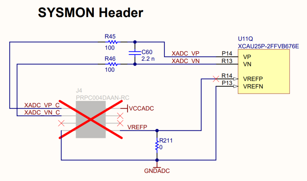
SYSMON
FPGA system monitor signals are available on a dedicated, non-populated 8-pin header at J4. The ADC signals are filtered through a simple RC network.
VREFP may optionally provide a precision reference for optimal performance of the ADC. See AMD UG580 UltraScale Architecture System Monitor for additional details.
| J4 pin | Connection |
|---|---|
| 1 | XADC_VP_C (FPGA P14) |
| 2 | VCCADC (1.8V supplied by the XEM8320) |
| 3 | XADC_VN_C (FPGA R13) |
| 4 | Not Connected |
| 5 | Not Connected |
| 6 | Not Connected |
| 7 | VREFN (FPGA P13) |
| 8 | VREFP (FPGA R14) |