BRK1900 Breakout Board
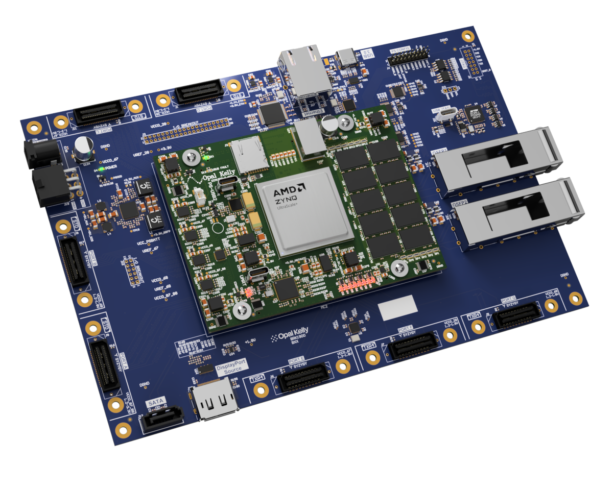
The BRK1900 is a complete reference platform for the ECM1900 Edge Compute Module™ providing multiple interfaces to various connections on the ECM1900 such as DC power input, 7x SYZYGY connectors, QSFP receptacles, a SATA connector, JTAG, ethernet PHY, USB PHY, and a programmable clock oscillator. Three additional 2mm headers provide connections to the remaining FPGA and CPU I/O pins for general purpose application.
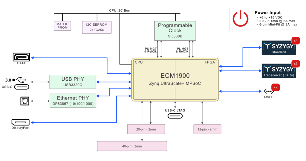
Functional Block Diagram
Powering the BRK1900
The BRK1900 requires a clean, filtered, DC supply within the range of 6 V to 15 V. This supply is passed directly to the ECM1900 as well as being used for onboard regulators. It may be delivered in one of two ways:
- 6-pin Mini-Fin connector – Pins 1, 2, and 3 are tied to the input supply net +VDCIN. Pins 4, 5, and 6 are tied to ground. The total maximum current allowed over this connector is 8 A. The part number is Molex 0455580003. The mating plug part number is Molex 0455590002. Several options for crimping pins are available, including Molex 0039000038. While it is possible to provide power using a commercial PC power supply with compatible pinout, it is recommended to create a custom cable harness for use with an appropriate bench supply.
- DC barrel jack – The jack is part number PJ-102AH from CUI, Inc. It is a standard “canon-style” 2.1mm / 5.5mm jack. The total maximum current allowed over this connector is 5 A. The outer ring is connected to DGND. The center pin is connected to +VDCIN.
Please refer to Powering the ECM1900 for information on the ECM1900 power systems.
LED Indicators
The BRK1900 includes two LED indicators for power status.
| LED | Designator | ON CONDITION |
|---|---|---|
| BRK1900 Power Good | D4 | Power good indicator for the BRK1900 power rails |
| VBUS FAULT | D1 | Power output fault for the host 3.0 type-c USB port |
Peripherals
The ECM1900 Pin List has full connection information in the “BRK1900” columns. Additionally, please refer to the schematics and layout available on the Pins downloads page for detailed connection diagrams.
Peripheral Bank Connections
The table below summarizes the various connectors on the BRK1900. The ECM1900 Pin List has connection information in the “BRK1900” column. Additionally, please refer to the schematics and layout available online for detailed connection diagrams.
| CONNECTOR TYPE | FPGA BANK |
|---|---|
| SYZYGY Standard Port A | 87-88 |
| SYZYGY Standard Port B | 68 |
| SYZYGY Standard Port C | 67 |
| SYZYGY Standard Port D | 28 |
| SYZYGY Transceiver (TXR-4) Port E | 67, GTH 225 |
| SYZYGY Transceiver (TXR-4) Port F | 28, GTH 224 |
| SYZYGY Transceiver (TXR-4) Port G (Rev BXX+) | 68, GTH 223 |
| QSFP #1 | 87, GTH 227 |
| QSFP #2 | 87, GTH 226 |
| FPX | GTH 223 |
| USB 3 | 502, GTR 505 |
| Ethernet | 500, 501, 502 |
| SATA | GTR 505 |
| DisplayPort | GTR 505, 67 |
| 2mm Breakout | 500, 68 |
SYZYGY Ports
For information on the SYZYGY ports see the BRK1900 SYZYGY Ports page.
Ethernet PHY
The Ethernet PHY onboard the BRK1900 supports the RGMII and MDC/MDIO user interface as well as 10Base-T, 100Base-TX, and 1000Base-T standards. It is connected to the hard processor system (PS) on the Zynq UltraScale+ at the MIO pin locations listed under BRK1900 ZYNQMP Configuration. The processor system will control this PHY directly. If you would like to access this PHY from the PL, you can set up the PL to master an AXI master-slave communication link with the PS MAC core. Further information regarding this arrangement can be found within Xilinx documentation.
| REVISION | ETHERNET PHY |
|---|---|
| AXX | Microchip KSZ9031RNXCA |
| BXX+ | Ti DP83867IRPAP |
QSFP Transceiver Cages
The BRK1900 has two QSFP cages installed, but require transceivers to be used. The following Ethernet fiber optic transceiver is one option.
| MANUFACTURER | PART NUMBER | DESCRIPTION | APPROXIMATE COST |
|---|---|---|---|
| 10Gtek | AMQ10-SR4-M1 | 40GBASE-SR4 QSFP+ Transceiver for MMF, 100M | $39.00 / each |
DisplayPort – Processing System (PS) Side
The Processing System (PS) side DisplayPort is connected to lanes 0-1 of the GTR transceivers. The AUX channel and the hot plug detect channel are to be connected through EMIO. The connection locations for these signals are given below:
The Processing System (PS) side DisplayPort is only supported with BRK1900 revision BXX and newer. It is not supported on revision AXX.
| SIGNAL | FPGA PIN | FPGA BANK |
|---|---|---|
| Hot Plug Detect | J17 | 67 |
| AUX_P | G18 | 67 |
| AUX_N | F18 | 67 |
USB 3.0 Type-C Host
The BRK1900 includes a USB 3.0 host port using a Type-C connector. The USB SuperSpeed lanes are connected to one set of the PS 505 transceiver lanes. The USB 2.0 connection is provided by a Microchip USB3320C-EZK PHY connected to PS 502 MIO pins. Port current output is limited by a Diodes Incorporated AP22653AW6-7 current limiter. See the BRK1900 schematic for more connection details.
I2C Peripherals
Several I2C devices add functionality to the BRK1900 to help implement a complete system. These are summarized in the table below:
| PART NUMBER | DESIGNATOR | I2C ADDRESS | FUNCTION |
|---|---|---|---|
| Microchip 24AA025E48-I/SN | U15 | 1010 111x | Ethernet MAC ID PROM |
| Microchip 24FC256-I/SN | U1 | 1010 100x | IPMI EEPROM (256 KB) |
| Texas Instruments HD3SS3220RNH | U14 | 1100 111x | USB Type-C controller with MUX |
| Texas Instruments TPS65400RGZ | U19 | 1101 001x | 4-channel switching regulator for BRK1900 periperhals |
| Silicon Labs SI5338B-B-GM | U2 | 1110 000x | Programmable Clock Oscillator |
2mm I/O Headers
Otherwise unused I/O are broken out into banks of 2mm headers. The headers pins are unpopulated by default.
For full I/O connection details see the ECM1900 Pin List.
| HEADER DESIGNATOR | PIN COUNT | CONNECTED BANKS | OTHER |
|---|---|---|---|
| J3 | 20 I/O 20x GND | 500 | XADC_VP, XADC_VN, POR_OVERRIDE |
| J4 | 0 I/O 9x GND, 1x 1.8V | PSCONFIG signals | |
| J10 | 6 I/O 6x GND | 68 |
PSCONFIG
The expansion header J4 includes the PSCONFIG signals. A 2mm male header is included to connect to the signals and to place jumpers to set the PS boot mode. For more information see Zynq UltraScale+ TRM (UG1085). Table 11-1: Boot Modes lists the boot mode options for the PSMODE pins.
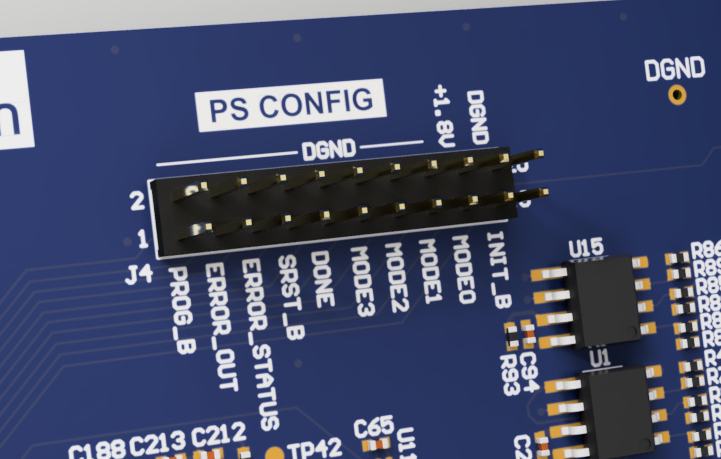
| J4 Pin | Signal | Note |
|---|---|---|
| 1 | PS_PROG_B | Pull-Up on ECM1900 |
| 3 | PS_ERROR_OUT | |
| 5 | PS_ERROR_STATUS | |
| 7 | PS_SRST_B | Pull-Up on ECM1900 |
| 9 | PS_DONE | Pull-Up on ECM1900 |
| 11 | PS_MODE3 | Pull-Up on ECM1900 |
| 13 | PS_MODE2 | Pull-Up on ECM1900 |
| 15 | PS_MODE1 | Pull-Up on ECM1900 |
| 17 | PS_MODE0 | Pull-Down on ECM1900 |
| 19 | PS_INIT_B | Pull-Up on ECM1900 |
| 2, 4, 6, 8, 10, 12, 14, 16, 20 | DGND | |
| 18 | +1.8V |
JTAG
The BRK1900 (revision BXX+) has a built in USB JTAG adapter. Connect to the USB-C connector J21 for AMD tools compatible access to the ECM1900’s JTAG interface.
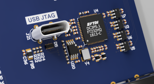
The JTAG connections are also wired to a dedicated 2mm header J2 that can be used with a compatible JTAG cable. The JTAG interface presented is at a 1.8V signaling voltage. This header is not populated by default. This footprint is compatible with the Molex part 87831-1420.
| CONNECTOR PIN | JTAG SIGNAL | CONNECTOR PIN | JTAG SIGNAL |
|---|---|---|---|
| 1 | GND | 2 | +1.8V (Vref) |
| 3 | GND | 4 | JTAG_TMS |
| 5 | GND | 6 | JTAG_TCK |
| 7 | GND | 8 | JTAG_TDO |
| 9 | GND | 10 | JTAG_TDI |
| 11 | GND | 12 | NC |
| 13 | GND | 14 | NC |
Programmable Clock Oscillator
This clock oscillator is separate and not synchronous to the clock provided by the USB host interface.
An Si5338B programmable oscillator provides four independent LVDS clock pairs to the PS and PL of the MPSoC. All four are connected to transceiver reference clock inputs. The input reference for the Si5338B is a fixed-frequency 25-MHz crystal oscillator. The output frequency of each channel has a range of 0.16-350 MHz. See the Si5338B data sheet for more information on configuring this part.
The default frequencies used in the set-clock-brk1900 application are shown below. This application is baked into the provided BRK1900 Linux image. This application is automatically run during boot in the setclk-reboot-init initializer script. The Clock Builder Pro project file used to generate the configuration data is located on GitHub. You can use this ClockBuilder Pro project as a template for creating your own configuration files. You can follow the instructions at BRK1900 Linux Image to configure any desired default frequency available after boot.
Transceiver Reference
| SI5338B OUTPUT | DEFAULT FREQUENCY |
|---|---|
| CLK0 | 125 MHz |
| CLK1 | 26 MHz |
| CLK2 | 156.25 MHz |
| CLK3 | 156.25 MHz |
| SI5338B OUTPUT | FPGA PIN | FPGA PIN NAME |
|---|---|---|
| CLK0A (LVDS +) | P27 | PS_MGTREFCLK1P_505 |
| CLK0B (LVDS -) | P28 | PS_MGTREFCLK1N_505 |
| CLK1A (LVDS +) | M27 | PS_MGTREFCLK2P_505 |
| CLK1B (LVDS -) | M28 | PS_MGTREFCLK2N_505 |
| CLK2A (LVDS +) | U10 | PL_MGTREFCLK1P_226 |
| CLK2B (LVDS -) | U9 | PL_MGTREFCLK1N_226 |
| CLK3A (LVDS +) Rev AXX | AC10 | PL_MGTREFCLK1P_223 |
| CLK3B (LVDS -) Rev AXX | AC9 | PL_MGTREFCLK1N_223 |
| CLK3A (LVDS +) Rev BXX | R10 | PL_MGTREFCLK1P_227 |
| CLK3B (LVDS -) Rev BXX | R9 | PL_MGTREFCLK1N_227 |
Configuration Interface
| SI5338B | FPGA PIN |
|---|---|
| SCL | A28 (PS_MIO16) |
| SDA | C29 (PS_MIO17) |
| I2C Address | 1110 000x |
ECM1900 Mounting
The ECM1900 is not hot pluggable. Disconnect all power before mounting or unmounting the ECM1900 .
The ECM1900 uses multiple high pin count expansion connectors. Care must be taken when mounting and unmounting from the BRK1900. See the Jack Screw Instructions page for the proper mounting procedure.
Schematic and Design Files
The BRK1900 schematics and design files are available in the Downloads section of the Pins website.
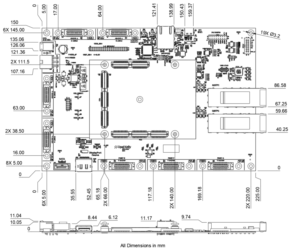
Mechanical Drawing
3D Models are available in SolidWorks, STEP, EASM and IGES formats.
Revision BXX