Powering the ECM1900
The ECM1900 requires a clean, filtered, DC supply within the range of 6 V to 15 V. This supply must be delivered through the mezzanine connector MC3. Using all 10 available pins, this connection has a maximum current rating of 20 A.
Power Supply
The ECM1900 is designed to be operated from a single 6-15 VDC power source supplied through mezzanine connector MC3. This provides for the several high-efficiency switching regulators on-board to provide multiple DC voltages for various components on the module as well as the user-adjustable I/O supplies.
Over-Voltage Protection and Under-Voltage Lockout
The ECM1900 includes an over-voltage protection circuit which disconnects the input supply from the on-board circuitry when the input is higher than approximately 15.7V. It is also prevented from powering on when the input supply is below approximately 4.5V. And it is protected from reverse polarity voltage connected to the input.
Power Supply Monitoring
Multiple voltage, current, and temperature sensors are available on the ECM1900. Please see the I2C Peripherals documentation for details on interfacing to these devices.
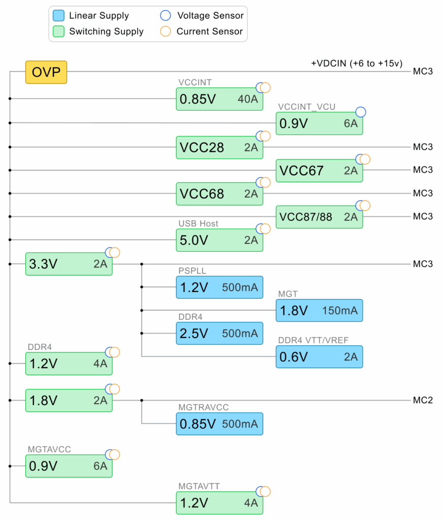
Power Distribution System Diagram
The ECM1900 power distribution system is quite complex, with several supplies designed to provide suitable, efficient power for several systems and modules. A schematic diagram of the system follows, with input (+VDC) shown to the left and accessible supply rails shown to the right.
VIO and VCCO I/0 Bank Associations
The VIO and VCCO naming associations and the I/O banks they power are as follows:
| VIO | VCCO | BANK | VOLTAGE RANGE |
|---|---|---|---|
| VIO1 | VCCO_87_88 | 87 & 88 | 1.2V – 3.3V |
| VIO2 | VCCO_68 | 68 | 1.2V – 1.8V |
| VIO3 | VCCO_67 | 67 | 1.2V – 1.8V |
| VIO4 | VCCO_28 | 28 | 1.2V – 1.8V |
The VIO are programmable voltage step down ICs that can be programmed on the ECM1900 using the ‘syzygy-ecm1900’ application that is baked into the provided Linux Images. The sources for this application be be found at the following GitHub repository: BRK1900 Applications
These VIO voltages will need to be enabled and programmed to the desired voltage to power these I/O banks if you desire to work with any of the VCCO rails or Bank I/O, both of which are connected to the MC connectors. You will need to determine the I/O bank of the pins you require by inspecting the ECM1900 Pins page and program the necessary VIO/VCCO to the correct voltage for your design.
You can determine which I/O bank an FPGA pin is connected to from the Pins page by selecting ‘Display Options’ then ‘I/O Bank’ or you may inspect the ‘PIN DESCRIPTION’ which will have the Bank located within its name. For example ‘B68_L1P’ is connected to Bank 68.
Power Budget
The table below can help you determine your power budget for each supply rail on the ECM1900. All values are highly dependent on the application, speed, usage, and so on. Entries we have made are based on typical values presented in component datasheets or approximations based on Xilinx power estimator results. Shaded boxes represent unconnected rails to a particular component. Empty boxes represent data that the user must provide based on power estimates.
The user may also need to adjust parameters we have already estimated (such as FPGA Vcco values) where appropriate. All values are shown in milliwatts (mW) unless otherwise indicated.
“PL” indicates the component is related to the “programmable logic” portion of the FPGA device. “PS” indicates the component is related to the “processing system”.
| COMPONENT(S) | 0.85 V | 0.90 V | 0.90 V | 1.2 V | 1.2 V | 1.8 V | 3.3 V | VCCO_28 | VCCO_67 | VCCO_68 | VCCO_87_88 |
|---|---|---|---|---|---|---|---|---|---|---|---|
| Programmable clock | 200 | 990 | |||||||||
| DDR4 VDD/VDDQ | 2,760 | ||||||||||
| DDR4 VTT Termination | 925 | ||||||||||
| USB 2.0 PHY | 55 | ||||||||||
| MicroSD card | 265 | ||||||||||
| PL VCCINT, VCCINT_IO, VCCBRAM | |||||||||||
| PS INTLP, INTFP, INTFP_DDR | |||||||||||
| PS VCCINT_VCU (7EV only) | |||||||||||
| PL MGTAVCC | 2,040 | ||||||||||
| PL MGTAVTT | 2,670 | ||||||||||
| PL MGTVCCAUX | 200 | ||||||||||
| PL VCCAUX, VCCAUX_IO | 1,450 | ||||||||||
| PL VCCO64 + VCCO65 (USB Host Interface) | 25 | ||||||||||
| PL VCCO_28 | |||||||||||
| PL VCCO64 + VCCO65 + VCCO66 (DDR4) | 250 | ||||||||||
| PL VCCO67 | |||||||||||
| PL VCCO68 | |||||||||||
| PL VCCO87 + VCCO88 | |||||||||||
| PS VCCO_PSIO0_500/501/502/503 | 35 | ||||||||||
| PS VCCO_PSIO4_504 (DDR4) | 810 | ||||||||||
Total (mW) | 2,040 | 2,670 | 4,750 | 2210 | 1,310 | ||||||
Available (mW) | 34,000 | 3,600 | 3,600 | 4,800 | 4,800 | 7,200 | 6,600 | 1,000 mA 0.8-1.8V | 1,000 mA 0.8-1.8V | 1,000 mA 0.8-1.8V | 1,000 mA 0.8-3.3V |
Example ECM1900-ZU7EG FPGA Power Consumption
Xilinx Power Estimator (XPE) version 2018.2.2 was used to compute the following power estimates for the VCCINT supply. These are simply estimates; your design requirements may vary considerably. The numbers below indicate approximately 80% utilization.
| COMPONENT | PARAMETERS | VCCINT POWER (MW) |
|---|---|---|
| Clock | 300 MHz GCLK, 250,000 fanout | 1,957 |
| Clock | 350 MHz GCLK, 150,000 fanout | 1,442 |
| Logic | 300 MHz, 50,000 logic LUTs, 25,000 shift registers, 25,000 distributed RAMs, 250,000 registers | 6,145 |
| Logic | 350 MHz, 40,000 logic LUTs, 150,000 registers | 3,393 |
| Logic | 667 MHz (DDR4), 60,000 logic LUTs | 3,196 |
| BRAM | 18-bit, 300 MHz, 250 block RAMs, 50% toggle rate | 203 |
| BRAM | 36-bit, 350 MHz, 150 block RAMs, 50% toggle rate | 284 |
| DSP | 500 MHz, 1500 slices, 12.5% toggle rate | 3,448 |
| GTH | 20 channels, 16.375 Gb/s | 1,004 |
| Misc. | DCM, PLL, VCCINT_IO, etc. | 500 |
| Total | 21,572 mW | |
| Available | 34,000 mW |