Specifications
| Host Interface | 2x USB 3.0 Type C, SuperSpeed FrontPanel Support |
| FPGA | XCKU060-1FFVA XCKU115-1FLVA available on special order |
| Memory | 4 GiByte DDR4, 72-bit wide data interface (ECC capable) |
| NV Memory | 2x 16 MiB System Flash 32 MiB FPGA Flash |
| Oscillator | Programmable, 0.16-350 MHz |
| FPGA I/O | 332 HP I/O (Banks 24, 25, 44, 45, 46, 47, 48) |
| FPGA MGT | 28 GTH Transceivers (up to 16.375 Gb for -3E speed) |
| Dimensions | 145mm x 85mm (5.71″ x 3.35″) |
| MINIMUM | TYPICAL | MAXIMUM | UNITS | |
|---|---|---|---|---|
| DC Input | +4.5 | – | +16 | VDC |
| DC Input Ripple | – | – | 50 | mVp-p |
| Operating Temperature | 0 | – | +70 | ºC |
| Operating Temperature (Extended Version) | 0 | – | +85 | ºC |
| Storage Temperature | -50 | 0 | +100 | ºC |
| Weight | 132 | grams | ||
| Oscillator Frequency (Programmable) | 0.16 | – | 350 | MHz |
| Oscillator Period Jitter | 10 | ps pk-pk | ||
| Oscillator Reference Crystal Freq. Stability | ±50 |
PCB Footprint
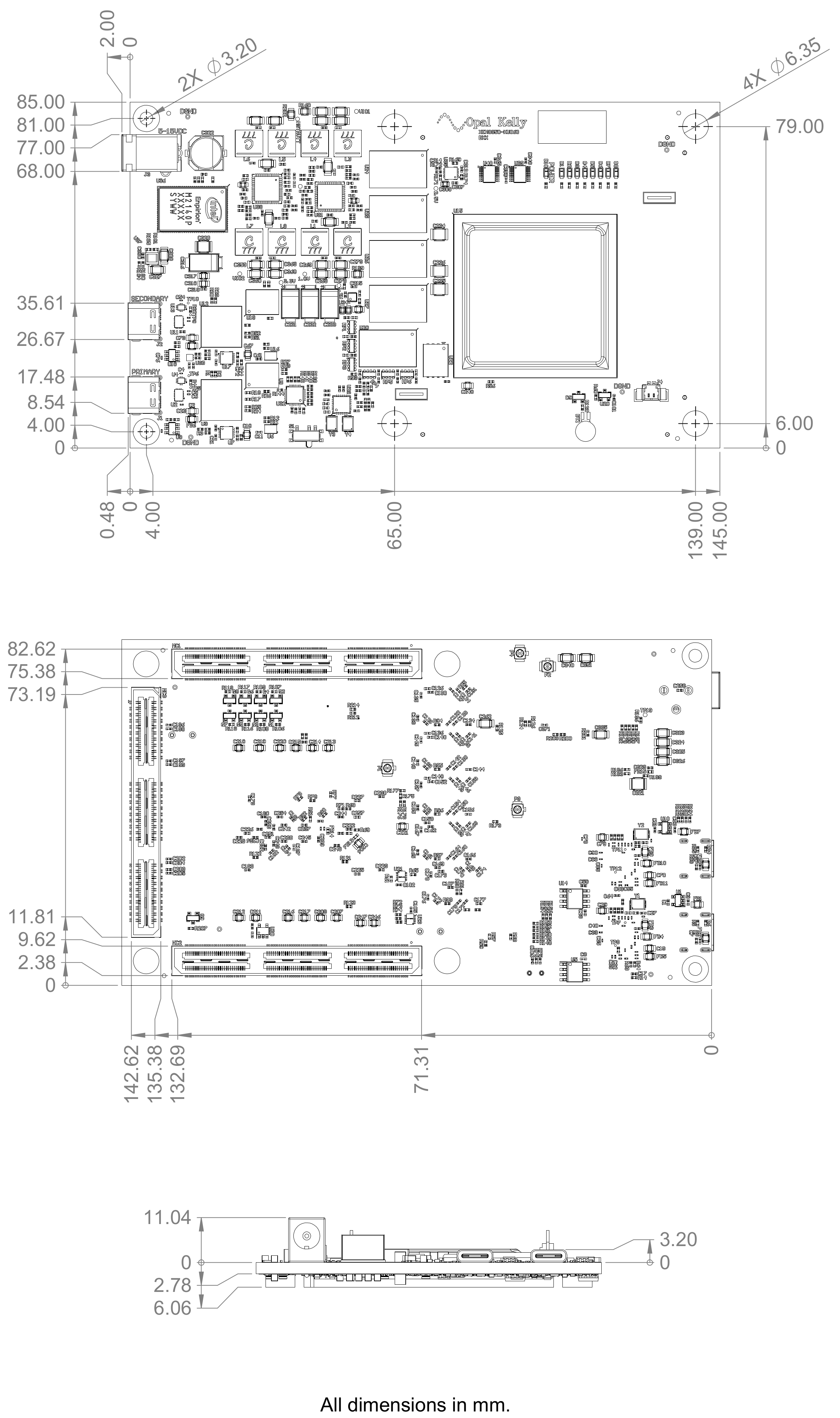
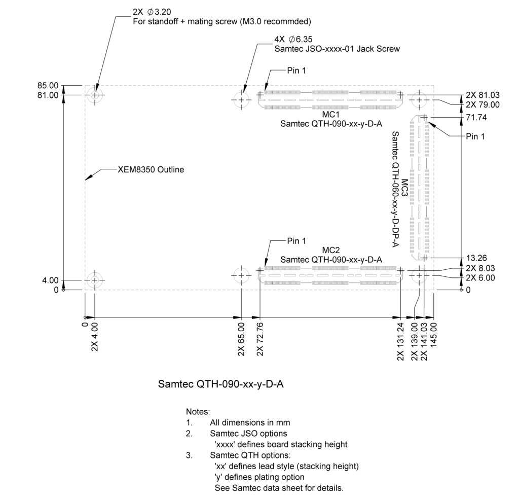
The PCB is 145mm x 85mm with six mounting holes spaced as shown in the drawings below. The four mounting holes adjacent to the mezzanine connectors accept Samtec JSO jack standoffs for controlled mating and unmating with a carrier board. The remaining two holes at the left side of the board accept size M3 mounting screws. The M3 mounting holes are plated through but are electrically isolated from all signals on the XEM8350. The JSO mounting holes are unplated. The three connectors (2x USB and DC power) overhang the PCB slightly in order to accommodate mounting within an enclosure.
The XEM8350 has three high-density 0.5mm connectors providing access to 332 I/O, 28 multi-gigabit transceivers, and multiple electrically-programmable adjustable voltages.
Mechanical Drawing
The mechanical drawing below may be used for enclosure or mounting hardware design. 3D Models are also available in SolidWorks, STEP, and IGES formats.

Mating Board Diagram
Use the mating diagram below to orient and design peripheral mating hardware. Note that this is a top-down view and mates to the bottom of the XEM8350. This design is realized in Altium CAD drawings in the corresponding breakout board which are available through Pins Downloads.
For Samtec connector details, drawings, models, and landing patterns, please visit Samtec’s website.

Heat Sink
The device has been fitted with two heat sink anchors, proximate to the FPGA for mounting a passive or active heat sink. The following heat sink has been tested with the XEM8350.
| MANUFACTURER | PART NUMBER | DESCRIPTION |
|---|---|---|
| Opal Kelly Incorporated | FANSINK-40X40 | Active heatsink with DC fan |
The active heat sink above includes a small fan which connects to the fan controller on-board for manual or automatic fan control. The fan is powered directly by the input supply to the XEM8350. The fan is specified for a nominal operating voltage of 6-13.8 VDC. Supply voltages outside of this range might be possible, but could lead to fan startup and performance issues under certain conditions. The fan is powered directly by the input supply, and therefore the maximum fan RPM is related to the external supply voltage. Designs with high FPGA on-chip power consumption must take this into account when selecting an operating voltage and heat sink.
The FANSINK-40X40 is available for purchase directly from Opal Kelly.
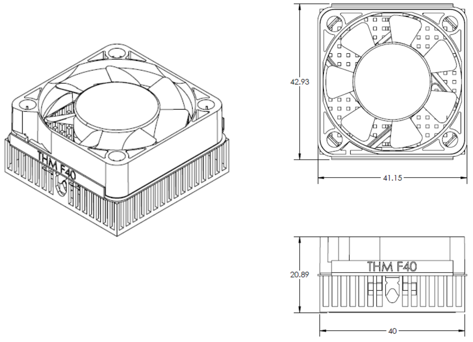
Heat Sink Dimensions

DIY Fansink Solution
The following components may be used to craft a suitable alternative for the FANSINK-40X40:
| Component | Digi-Key P/n | Description |
|---|---|---|
| Aavid 375024B60024G | Mouser 532-375024B60024 | Heatsink with anchor arms |
| CUI CFM-3510CF-190-277 | Mouser 179-CFM3510CF190277 Digi-Key 2223-CFM-3510CF-190-277-ND | Fan |
| McMaster-Carr 92196A235 | McMaster-Carr 92196A235 | Mounting bolt |
| Molex 510210200 | Mouser 538-51021-0200 Digi-Key WM1720-ND | Power connector |
| Molex 500798xxx | Digi-Key WM25388CT-ND | Crimp terminals |
| Molex 500798xxx | Digi-Key WM15250-ND | Pre-crimped cable assemblies |