LEDs
In addition to the power LED, there are eight LEDs, each of which is controlled by FPGA pins as shown in the table below.
| LED | FPGA PIN |
|---|---|
| D1 | AK22 |
| D2 | AM20 |
| D3 | AL22 |
| D4 | AL20 |
| D5 | AK23 |
| D6 | AJ20 |
| D7 | AL23 |
| D8 | AJ21 |
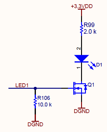
The LED anodes are connected through a current limiting resistor to +3.3 V and the cathodes wired through NMOS transistors to the FPGA I/O on Bank 44 with a bank voltage set by VIO2. To turn ON an LED, the FPGA pin should be at logic ‘1’. To turn OFF an LED, the FPGA pin should be at logic ‘0’.
VIO2 Compatibility
The I/O voltage for Bank 44 is set by VIO2 which is controlled by Device Settings. By default, this is disabled. In order to operate the LEDs, you must set this setting to an appropriate voltage (between 1.2V and 1.8V). The FET circuit described above effectively provides voltage translation and allows the LEDs to work with any supported voltage.