SZG-MULTIDAQ
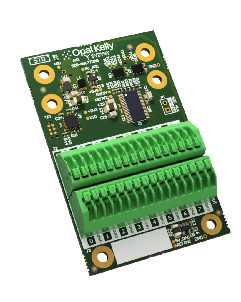
The SZG-MULTIDAQ is an analog instrumentation peripheral with 8 analog inputs and 8 analog outputs. It features a Texas Instruments ADS8688A 16-bit ADC and a Texas Instruments DAC80508 16-bit DAC. Spring loaded terminal blocks allow easy connection for input and output wires. This module is an excellent choice for analog input/output instrumentation and control needs.
Resources
- Aligni PLM – See the Attachments tab for schematics.
- SYZYGY Specification
- SYZYGY GitHub Site – Several projects that could be helpful.
- SZG-MULTIDAQ Example Design
- Product Page
Design
ADC / DAC Components
| PART | Designator | MANUFACTURER | PART NUMBER | Note |
|---|---|---|---|---|
| ADC | U1 | Texas Instruments | ADS8688AIDBT | 16-bit, 500-ksps, 8-channel SAR ADC with bipolar inputs using 5-V supply and low-drift VREF |
| DAC | U6 | Texas Instruments | DAC80508ZRTE | True 16-bit, 200-ksps, 8-channel, SPI, voltage-output DAC with precision internal reference |
Power
Both the ADC and DAC components require and accurate and low noise 5V rail. To provide this from the available SYZYGY power rails, a 5.5V boost regulator is first used, followed by an ultra low noise 5V linear regulator to supply each analog component.
| PART | Designator | MANUFACTURER | PART NUMBER |
|---|---|---|---|
| 5.5V Boost | U2 | Microchip | MCP1640BT-I/MC |
| 5V Linear Regulator | U3 and U5 | Texas Instruments | TPS7A2050PDBVR |
Data Interface
The SZG-MULTIDAQ is provided as a Standard SYZYGY port peripheral. The ADC and DAC utilize independent 4 wire SPI bus interfaces for data transfer and control. The data interface is level shifted from the SYZYGY ports VIO voltage to the 3.3V needed by the ADC and DAC interfaces so that a wide range of I/O voltages can be used. See the SYZYGY compatibility table below for the allowed VIO range.
ADC Port Connections
| SYZYGY PORT PIN | SIGNAL NAME | TYPE | DESCRIPTION |
|---|---|---|---|
S0 | ADC_SDI_C | Input | Data In |
S2 | ADC_SDO_C | Output | Data Out |
S4 | ADC_SCLK_C | Input | Data Clock |
S6 | ADC_CS_N_C | Input | Chip Select |
S8 | ADC_RST | Input | Reset |
ADC_RST is active high. When not driven, is not asserted.
DAC Port Connections
| SYZYGY PORT PIN | SIGNAL NAME | TYPE | DESCRIPTION |
|---|---|---|---|
S1 | DAC_SDI_C | Input | Data In |
S3 | DAC_SDO_C | Output | Data Out |
S5 | DAC_SCLK_C | Input | Data Clock |
S7 | DAC_CS_N_C | Input | Chip Select |
Connectors
The ADC and DAC outputs are each connected to a 16 pin spring contact terminal block. Press down on the spring lever while inserting or removing wires from the block. Every other pin on each connector is Ground. J2 has the ADC analog output pins and J3 has the DAC analog input pins.
| PART | MANUFACTURER | PART NUMBER |
|---|---|---|
| J2 and J3 | Phoenix Contact | 1990148 |
SYZYGY Information
Compatibility Table
| COMPATIBILITY PARAMETER | SPECIFICATION |
|---|---|
| Port type | SYZYGY Standard |
| Width | Single |
| 5V supply required | Yes |
| Nominal 5V supply current | 100 mA |
| Nominal 3.3V supply current | 100 mA |
| VIO supply voltage | 1.0V – 3.3V |
| Nominal VIO supply current | 10 mA |
| Total number of I/O | 9 |
| Number of differential I/O pairs | 0 |
DNA Data
| DNA PARAMETER | DATA |
|---|---|
| Max 5V Load | 100 mA |
| Max 3.3V Load | 100 mA |
| Max VIO Load | 10 mA |
| IS_LVDS | False |
| IS_DOUBLEWIDE | False |
| IS_TXR4 | False |
| VIO Range(s) | [1.0,3.3] |
Pinout
The source of the following pinout information is the SZG-MULTIDAQ schematic. This pinout follows the SYZYGY specification for Standard ports.
- Column PIN NUM (J1) lists the pin number on the SYZYGY specification’s Standard Samtec connector, this is reference designator J1 in the schematic.
- Column SIGNAL NAME lists the SYZYGY specification’s name for this pin’s connection.
- Column SCHEMATIC NET lists the net name found in the SZG-MULTIDAQ’s schematic for the connection.
| PIN NUM (J1) | SIGNAL NAME | SCHEMATIC NET | NOTE |
|---|---|---|---|
| 5 | S0 | ADC_SDI_C | |
| 6 | S1 | DAC_SDI_C | |
| 7 | S2 | ADC_SDO_C | |
| 8 | S3 | DAC_SDO_C | |
| 9 | S4 | ADC_SCLK_C | |
| 10 | S5 | DAC_SCLK_C | |
| 11 | S6 | ADC_CS_N_C | |
| 12 | S7 | DAC_CS_N_C | |
| 13 | S8 | ADC_RST | Can be left floating if not required |