SYZYGY ADC IP Core
Overview
This free core drives the Opal Kelly SZG-ADC-LTC226X peripheral.
- AXI4-Stream output. A 32-bit interface carrying one sample per channel.
- Customizable sample rate. The sample rate is set by the clock driven into
adc_sample_clk, up to 125 MSPS. - Automatic capture phase alignment. The LVDS data eye is centered at bring-up and can be set to run continuously. The phase alignment uses the Ultrascale+ IDELAY3 blocks and the eye characteristics can be read in status registers.
- AXI4-Lite or discrete ports. Select between a control and status register interface and standalone operation from discrete ports.
- SPI register access. In AXI4-Lite mode the converter’s full SPI register space is mapped into the address map.
Access the core at the OpalKelly design resources repository.
Core Information
| Channels | 2 |
| Resolution | 12-bit or 14-bit |
| Sample rate | Up to 125 MSPS |
| Sample output | AXI4-Stream, 32-bit |
| Control | AXI4-Lite, or discrete wires |
| Device family | Artix UltraScale+ |
Note: The core supports the Vivado board flow. Selecting the SYZYGY port the peripheral is fitted to on the szg_adc_interface board interface generates the pin constraints for the peripheral connections.
Core Customization
| Parameter | Default | Range | Description |
|---|---|---|---|
CTRL_INTERFACE | 0 | 0, 1 | Control and status interface: 0 = AXI4-Lite, 1 = discrete ports. |
ADC_VARIANT | 1 | 0, 1 | Peripheral variant: 0 = LTC2264-12, 1 = LTC2268-14. |
FIFO_DEPTH | 1024 | 16–131072 | Depth of the buffer carrying samples between the capture and stream clock domains. |
ALIGN_MODE | 0 | 0, 1 | Alignment mode: 0 = one-shot, 1 = continual. |
Interfaces and Signals
Bus Interfaces
| Interface | Type | Domain | Notes |
|---|---|---|---|
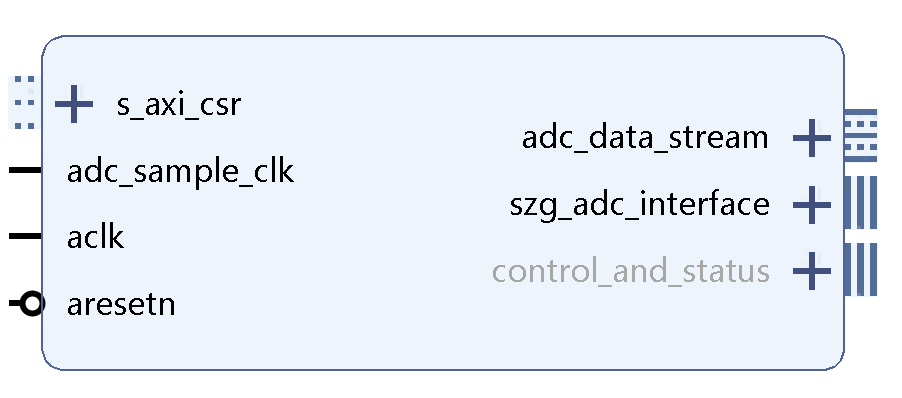
adc_data_stream | AXI4-Stream master | aclk | 32-bit continuous sample stream. |
s_axi_csr | AXI4-Lite slave | aclk | Present when CTRL_INTERFACE = 0. |
control_and_status | discrete ports | aclk | Present when CTRL_INTERFACE = 1. |
szg_adc_interface | custom | mixed | Make external to connect to SZG-ADC-LTC226X. |
Clocks and Resets
| Port | Dir | Description |
|---|---|---|
aclk | in | System clock. |
aresetn | in | Active-low system reset for the whole core. |
adc_sample_clk | in | Encode clock source. Frequency determines sample rate. |
Peripheral Connections
| Port | Dir | Description |
|---|---|---|
adc_data_1p, adc_data_1n [1:0] | in | Channel 1 serial data lanes. |
adc_data_2p, adc_data_2n [1:0] | in | Channel 2 serial data lanes. |
adc_dco_p, adc_dco_n | in | Data clock from the converter. Clocks the capture path. |
adc_fr_p, adc_fr_n | in | Frame clock from the converter. |
adc_encode_p, adc_encode_n | out | Encode clock to the converter. |
adc_sclk | out | SPI clock. |
adc_sdi | out | SPI data to the converter. |
adc_sdo | in | SPI data from the converter. |
adc_cs_n | out | SPI chip select, active-low. |
Discrete Control and Status (CTRL_INTERFACE = 1)
| Port | Dir | Description |
|---|---|---|
ctrl_realign | in | Pulse high for one cycle to re-run bring-up: the capture path is reset and re-aligned and the sample FIFO is flushed. |
ctrl_stream_en | in | Level. Gates the stream output. High out of reset. |
ctrl_clear_flags | in | One-cycle strobe. Clears the sticky flags. |
adc_ready | out | Bring-up complete. |
capture_clk_alive | out | The converter’s data clock is toggling. |
align_done | out | Eye centering finished. |
align_fail | out | Eye centering found no usable window. |
fifo_overflow | out | Sticky overflow. |
frame_error | out | Sticky frame error. |
align_phase [15:0] | out | Delay tap the eye sweep selected. |
eye_width [15:0] | out | Width of the eye it found, in delay taps. |
Register Map
Offsets are bytes from the s_axi_csr base. Any other offset in the block answers DECERR.Address Map
| Offset | Name | Access | Description |
|---|---|---|---|
0x00 | CTRL | RW | Action bits and the stream enable. |
0x04 | STATUS | RO | Ready, alignment, fault, and SPI state. |
0x08 | ALIGN | RO | Eye-center and width. |
0x40 – 0x5C | LTC226x registers | RW | Direct map of the converter register space. |
CTRL (0x00)
| Bit | Field | Description |
|---|---|---|
[0] | realign | Write-1-pulse. Capture path is reset and re-aligned and the sample FIFO is flushed. |
[2] | stream_enable | Gates the stream output. Set out of reset. |
[8] | clear_flags | Write-1-pulse. Clears error flags. |
[9] | spi_reconfig | Write-1-pulse. Re-applies every converter register written since reset. |
STATUS (0x04)
| Bit | Field | Description |
|---|---|---|
[0] | adc_ready | Capture is running and eye centering has completed. |
[1] | capture_clk_alive | The converter’s data clock is toggling. |
[2] | align_done | Eye centering finished. |
[3] | align_fail | Eye centering found no usable window. |
[4] | fifo_overflow | Sticky. The sample FIFO was full and samples were dropped. |
[5] | adc_spi_ready | The SPI engine is ready for register access. |
[6] | spi_busy | The SPI engine or sequencer is active, work is queued, or a register read is outstanding. |
[7] | frame_error | Sticky. The frame pattern stopped matching after alignment parked. |
ALIGN (0x08)
| Bits | Field | Description |
|---|---|---|
[15:0] | align_phase | Current eye center tap. |
[31:16] | eye_width | Current width of the eye in taps. |
LTC226x Register Map (0x40 – 0x5C)
Refer to the LTC2264/LTC2268 datasheet for the register contents.
Application Information
Sample Format
Each beat carries one sample per channel, MSB-aligned in its half-word, in signed two’s complement. Both channels sample on the same clock cycle.
| Bits | Meaning |
|---|---|
m_axis_tdata[31:16] | Channel 1 sample |
m_axis_tdata[15:0] | Channel 2 sample |
Note: Sample data out of the converter is in the adc_sample_clk domain and the stream is in the AXI aclk domain. If aclk is slower than adc_sample_clk, the core may overflow. Samples that arrive with the FIFO full are dropped and STATUS[4] latches.
Converter Configuration
The core applies no converter configuration at reset; the peripheral runs on its power-on defaults. Registers written through the address map are re-applied by an spi reconfigure call and discarded by a reset.
Release Notes
SYZYGY ADC IP 1.0
- Initial Release