SZG-ADC-LTC226X
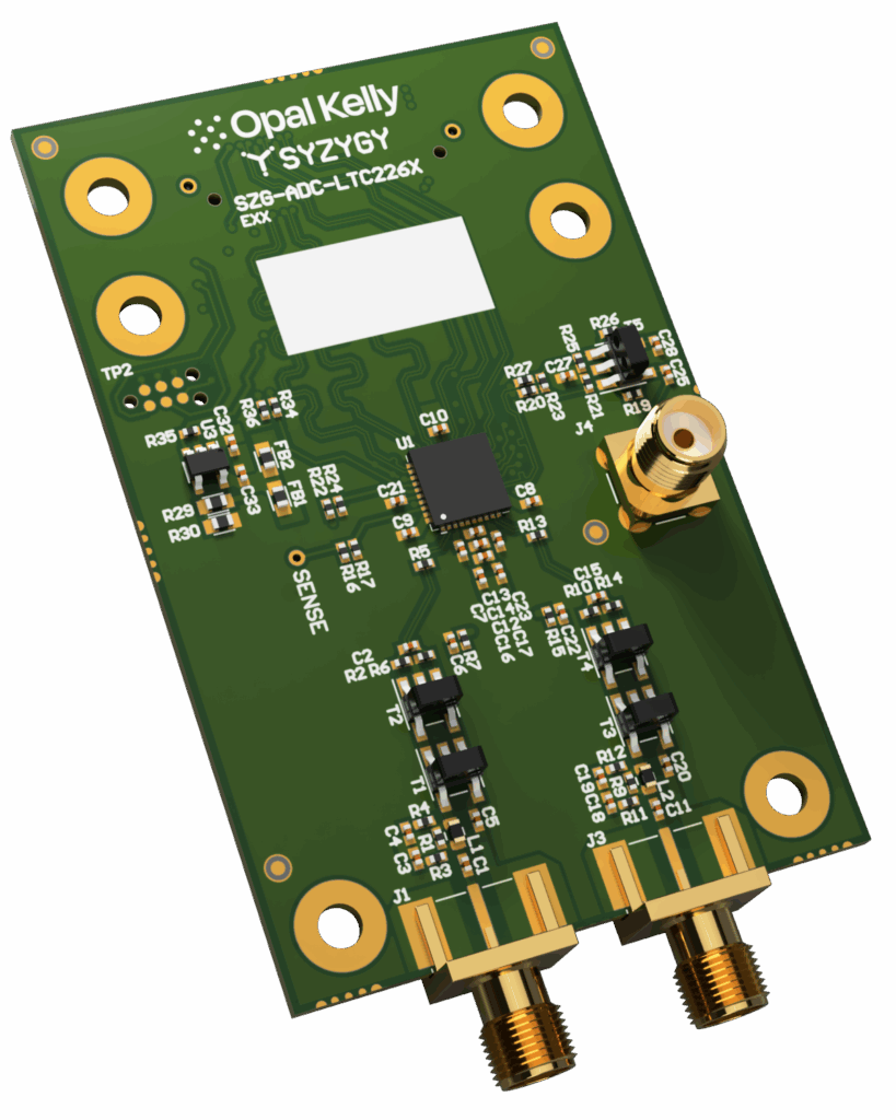
The SZG-ADC-LTC226X is a 2-channel ADC based on the Analog Devices LTC226X ADCs. The converter module is perfect for high-performance communications applications and general high-speed data acquisition.
The module is configured to accept a conversion clock from the FPGA on the carrier or (with user-applied resistor changes) a single-ended clock delivered by an on-board SMA connector.
Resources
- Aligni PLMs – See the Attachments tab for schematics
- SYZYGY Specification
- SYZYGY GitHub Site – Several projects that could be helpful
- SZG-ADC-LTC226X Example Design
- Product Page
SYZYGY Information
Compatibility Table
| COMPATIBILITY PARAMETER | SPECIFICATION |
|---|---|
| Port type | SYZYGY Standard |
| Width | Single |
| 5V supply required | No |
| Nominal 5V supply current | 0mA |
| Nominal 3.3V supply current | 500mA |
| VIO supply voltage | 1.2V to 3.3V |
| Nominal VIO supply current | < 10mA |
| Total number of I/O | 15 |
| Number of differential I/O pairs | 5 |
DNA Data
This data is stored in the SYZYGY DNA microcontroller on the SZG-ADC-LTC226X peripheral.
| DNA PARAMETER | DATA |
|---|---|
| Max 5V Load | 0 mA |
| Max 3.3V Load | 500 mA |
| Max VIO Load | 10 mA |
| IS_LVDS | True |
| IS_DOUBLEWIDE | False |
| VIO Min | 1.2V |
| VIO Max | 3.3V |
Pinout
The source of the following pinout information is the SZG-ADC-LTC226X schematic. This pinout follows the SYZYGY specification for STD ports.
- Column
PIN NUM (J1)lists the pin number on the SYZYGY specification’s Standard Samtec connector, this is reference designator J1 in the schematic. - Column
SIGNAL NAMElists the SYZYGY specification’s name for this pin’s connection. - Column
SCHEMATIC NETlists the net name found in the SZG-ADC-LTC226X’s schematic for the connection.
| PIN NUM (J1) | SIGNAL NAME | SCHEMATIC NET |
|---|---|---|
| 5 | D0P | OUT1A+ |
| 7 | D0N | OUT1A- |
| 6 | D1P | FR+ |
| 8 | D1N | FR- |
| 9 | D2P | OUT1B+ |
| 11 | D2N | OUT1B- |
| 10 | D3P | OUT2A+ |
| 12 | D3N | OUT2A- |
| 13 | S8 | SDO |
| 14 | D5P | OUT2B+ |
| 16 | D5N | OUT2B- |
| 15 | S10 | CS_B |
| 17 | S12 | SCLK |
| 19 | S14 | SDI |
| 33 | P2C_CLKp | DCO+ |
| 35 | P2C_CLKn | DCO- |
| 34 | C2P_CLKp | ENC+ |
| 36 | C2P_CLKn | ENC- |
Design
The design of the SZG-ADC-LT226X has been heavily influenced by the evaluation board designed and produced by Linear Technology (Analog Devices).
Linear Technology (Analog Devices) LTC226X
From the LTC226X datasheet:
The LTC® 2268-14/LTC2267-14/LTC2266-14 and the LTC®2265-12/LTC2264-12/LTC2263-12 are 2-channel, simultaneous sampling A/D converters designed for digitizing high frequency, wide dynamic range signals. The former is a 14-bit converter with an AC performance of 73.1dB SNR and 88dB SFDR, while the latter is a 12-bit converter with an AC performance of 71dB SNR and 90dB SFDR. Both have ultralow jitter of 0.15psRMS, allowing undersampling of IF frequencies with excellent noise performance. The DC specs for the LTC® 2268-14/LTC2267-14/LTC2266-14 include ±1LSB INL (typ), ±0.3LSB DNL (typ), and no missing codes over temperature. The transition noise is a low 1.2LSB RMS. The DC specs for the LTC®2265-12/LTC2264-12/LTC2263-12 include ±0.3LSB INL (typ), ±0.1LSB DNL (typ), and no missing codes over temperature. The transition noise is a low 0.3LSB RMS
The digital outputs are serial LVDS to minimize the number of data lines. Each channel outputs two bits at a time (2-lane mode) or one bit at a time (1-lane mode). The LVDS drivers have optional internal termination and adjustable output levels to ensure clean signal integrity.
The ENC+ and ENC– inputs may be driven differentially or single-ended with a sine wave, PECL, LVDS, TTL, or CMOS inputs. An internal clock duty cycle stabilizer allows high performance at full speed for a wide range of clock duty cycles.
Analog Inputs
The applicable input frequency range of the SZG-ADC-LTC226X is approximately 5 MHz to 140 MHz. For optimal distortion and noise performance, or for input frequencies above 140 MHz, the RC networks on the analog inputs may need to be optimized. For optimal SNR performance, external filters may be required. Refer to the documentation below.
| PARAMETER | VALUE |
|---|---|
| Maximum analog input voltage | 2 Vpp* |
| Input impedance | 50 Ω |
* The input range may be adjusted using the SENSE pin on the LTC226x. Refer to the documentation below.
Encode Clock Input
By default, the SZG-ADC is configured to accept a differential clock over the C2P_CLK connection from the carrier. To apply an external single-ended clock over the SMA connector J4, remove resistors R18 and R28, and place resistors R20 and R27.
The encode clock inputs may be driven at any level up to 3.6 V. When driving the inputs using a differential signal, the negative input (ENC-) must stay at least 200 mV above circuit ground.
Additional Documentation
Product Lifecycle
PCB Revision History
| REVISION | DETAIL |
|---|---|
| EXX | Update SDO connection (see Known Issues) |
| DXX (20200309) | Solder mask updates for improved manufacturability |
| CXX (20190702) | Add MCU control of LDO |
| BXX (20171026) | Add SDO pullup |
| AXX (20170626) | Initial release |
Known Issues
Rev DXX
SDO Level Translator Incompatibility
The optional SDO connection in the SPI configuration interface is incompatible with the level translator. This means that the ADC’s configuration registers can be written to, but not read. Register read is only used to verify the written configuration, as there are no status or data registers available from that interface.
Rev EXX
SDO Accessibility
The SDO signal in the SPI configuration interface can be accessed under the following conditions:
- A 0-ohm 0402 resistor must be placed at reference designator location R36. This resistor connects the SDO pin on the LTC226X to the SYZYGY connector, pin 13.
- VIO must be within the range of 1.8-3.3V. SDO is an open-drain output from the LTC226X. It includes a 2.0-kΩ pullup resistor to VIO, and the pullup voltage must be within 1.8-3.3V for proper chip operation.