Expansion Connectors
Opal Kelly Pins is an interactive online reference for the expansion connectors on all Opal Kelly FPGA integration modules. It provides additional information on pin capabilities, pin characteristics, and PCB routing.
Pins can also generate constraint files (XDC) and help you map your HDL net names to FPGA pin locations automatically
Expansion Connectors
Two high-density 180-pin expansion connectors and one high data rate optimized 120-pin expansion connector are available on the bottom-side of the XEM8370 PCB. These expansion connectors provide user access to several power rails on the XEM8370, the JTAG interface on the FPGA, and dedicated I/O pins on the FPGA, including several global clock inputs. High-speed gigabit transceiver signals are also available through these expansion connectors. Each connector has a ground spine running its entire length for a solid reference ground connection.
The MC1 and MC3 connectors on the XEM8370 are Samtec part number: QSH-090-01-L-D-A. The table below lists the appropriate Samtec mating connectors along with the total mated height. The QTH-090-01-F-D-A part is used on the BRK8370 breakout board.
| SAMTEC PART NUMBER | MATED HEIGHT |
|---|---|
| QTH-090-01-F-D-A | 5.00mm (0.197″) |
| QTH-090-02-F-D-A | 8.00mm (0.315″) |
| QTH-090-03-F-D-A | 11.00mm (0.433″) |
| QTH-090-04-F-D-A | 16.00mm (0.630″) |
| QTH-090-05-F-D-A | 19.00mm (0.748″) |
| QTH-090-07-F-D-A | 25.00mm (0.984″) |
The MC2 connector on the XEM8370 is Samtec part number: QSH-060-01-L-D-DP-A. This connector has more isolation space between the differential pairs of the transceiver pins. The table below lists the appropriate Samtec mating connectors along with the total mated height. The QTH-060-01-L-D-DP-A part is used on the BRK8370 breakout board.
| SAMTEC PART NUMBER | MATED HEIGHT |
|---|---|
| QTH-060-01-L-D-DP-A | 5.00mm (0.197″) |
| QTH-060-02-L-D-DP-A | 8.00mm (0.315″) |
| QTH-060-03-L-D-DP-A | 11.00mm (0.433″) |
| QTH-060-04-L-D-DP-A | 16.00mm (0.630″) |
| QTH-060-05-L-D-DP-A | 19.00mm (0.748″) |
| QTH-060-07-L-D-DP-A | 25.00mm (0.984″) |
Jack Screw Standoffs
The XEM8370 uses Samtec Jack Screw Standoffs to ensure even mounting and un-mounting pressure when connecting to a base board. The table below lists the appropriate Samtec Jack Screw Standoffs along with the total mated height. The JSO-0515-01 part is used on the BRK83570 breakout board. Samtec Jack Screw Standoffs are sold as a set consisting of the base, jack screw, washer, and mounting screw. Four Jack Screw Standoffs are required to mount the XEM8370 to a base board.
| SAMTEC PART NUMBER | MATED HEIGHT | BASE BOARD CONNECTION STYLE |
|---|---|---|
| JSO-0515-01 | 5.00mm (0.197″) | Press fit |
| JSO-0815-01 | 8.00mm (0.315″) | Press fit |
| JSO-0815-03-L | 8.00mm (0.315″) | Threaded |
| JSO-1115-03-L | 11.00mm (0.433″) | Threaded |
| JSO-1615-03-L | 16.00mm (0.630″) | Threaded |
FPGA Bank Connections
Mezzanine connectors MC1, MC2, and MC3 are high-density connectors providing access to power, fabric I/O, transceivers, and several other signals. Pin mappings are listed on the Pins List. For more details about specific FPGA inputs and outputs, see AMD’s Kintex UltraScale+ documentation.
MC1 and MC3 are 180-pin connectors providing access to fabric I/O, GTY transceivers and the user-adjustable I/O supply rails VIO1, VIO2 and VIO3.
MC2 is a 120-pin connector with differential pair spacing. This connector provides access to the GTH transceivers on the FPGA, as well as the VDCIN connection, FPGA JTAG signals, XADC and VBATT connections, board power good and power enable signals, and the I2C interface used for SYZYGY SmartVIO applications.
| FPGA BANK | HR / HP | VOLTAGE RANGE(*) | MCX | VIO | VCCO Rail | I/O AVAILABLE |
|---|---|---|---|---|---|---|
| 64 | HP | 0.95 – 1.90 V | MC3 | VIO3 | VCCO_64_66 | 50 (including 4 GC pairs) |
| 66 | HP | 0.95 – 1.90 V | MC3 | VIO3 | VCCO_64_66 | 49 (including 4 GC pairs) |
| 67 | HP | 0.95 – 1.90 V | MC1/MC3 | VIO2 | VCCO_67_68_69 | 50 (including 4 GC pairs) |
| 68 | HP | 0.95 – 1.90 V | MC1 | VIO2 | VCCO_67_68_69 | 52 (including 4 GC pairs) |
| 69 | HP | 0.95 – 1.90 V | MC1 | VIO2 | VCCO_67_68_69 | 52 (including 4 GC pairs) |
| 88 | HD | 1.14 – 3.40V | MC3 | VIO1 | VCCO_88_89 | 24 (including 4 GC pairs) |
| 89 | HD | 1.14 – 3.40V | MC3 | VIO1 | VCCO_88_89 | 24 (including 4 GC pairs) |
Note: Voltage ranges specified here are the range supported by the FPGA bank itself, not the range of the power supply connected to the bank. For power supply ranges refer to Device Settings.
Setting the Adjustable I/O Voltages
Three programmable high-efficiency switching regulators are on the XEM8370 which control the three adjustable voltages VIO1, VIO2, and VIO3. These are connected to the FPGA bank VCCIO according to the tables above. There are two ways to set these voltages:
- Device Settings – The FrontPanel firmware supports separate non-volatile device settings that are used to set these voltages during the power-on sequence. You can manually program these using the FrontPanel API or the FrontPanel application. See the Device Settings page for information on configuring these voltages.
- Peripheral Personality EEPROM – You can program a small EEPROM on your peripheral (the device that attaches to the XEM8370 mezzanine connectors) that can tell the FrontPanel firmware how to configure these voltages during the power-on sequence. See below for additional information.
Note: Changes to VIO settings require a power cycle to take effect.
Peripheral Personality EEPROM
During power-on sequencing the device firmware will query an I2C EEPROM at address 0xA2 1010 001x. This EEPROM would be connected to FX3_SDA_1V8 (MC2 pin 16) and FX3_SCL_1V8 (MC2 pin 14) and uses 1.8V logic levels. If present, the firmware will attempt to read an IPMI-formatted block of data that tells it how to configure the three adjustable voltage regulators.
Opal Kelly has provided an online tool to generate the contents of this EEPROM. Simply enter the details of your product into the online form to generate a binary file that can be stored on your EEPROM. The FrontPanel application can be used to program the generated binary file into the EEPROM.
Connector Mating
The three connectors on the XEM8370 are high-density, precision connectors and require considerable forces for mating and un-mating. To prevent damage to the carrier or peripheral boards, jack screw mounting hardware is used. Please review and follow the Jack Screw Instructions when mating and un-mating.
Fan Power Supply
A 3-pin connector (Molex 22-23-2031) at J2 provides power to an optional fansink for FPGA cooling. This fan is controlled by a digital fan controller as part of the Device Sensors and Device Settings capabilities. Please see the Device Settings section for details on controlling the fan.
The fansink is powered directly by the +VDCIN input voltage to the XEM8370. The allowable range for +VDCIN is 5-18 VDC. When utilizing the Opal Kelly FANSINK-07, it is recommended to use an input +VDCIN voltage within the specified operating range of the fansink: 10.8 to 13.2 VDC.
Additional fansink information is available on the FanSink page.
| PIN | SIGNAL |
|---|---|
| 1 | Tachometer (Not Used) |
| 2 | +VDCIN |
| 3 | GND |
Note: On XEM8370 PCB revision AXX the pin 1 silk indicator is mislabeled, it is in fact pin 3.
SYSMON
The AMD Kintex UltraScale+ SYSMON ADC input feature is routed through two 100Ω resistors to the MC2 connector. There is a 2.2 nF capacitor installed across the two FPGA pins for decoupling.
VREFP is routed to an MC2 pin. By default it is decoupled with a 0.1uF capacitor and ready for an external reference voltage. If desired, a 0Ω jumper can be placed on R185 to connect VREFP to ground, which will enable the internal voltage reference.
VCCADC and GNDADC are also routed to MC2 pins. They are connected to +1.8V and DGND though ferrite beads FB7 and FB8, respectively. There are two capacitor across the VCCADC and GNDADC pins on the FPGA, a 0.1uF and a 0.47uF.
| FPGA FUNCTION | FPGA PIN | MC2 PIN | Related REFDES |
|---|---|---|---|
| ADC_VP | V12 | 10 | R36 |
| ADC_VN | W11 | 12 | R37 |
| VREFP | W12 | 27 | C253, R185 |
| VCCADC | U12 | 26 | FB7 |
| GNDADC | U11,V11 | 28 | FB8 |
Considerations for Differential Signals
The XEM8370 PCB layout and routing has been designed with several applications in mind, including applications requiring the use of differential (LVDS) pairs. Please refer to the AMD Kintex UltraScale+ datasheet for details on using differential I/O standards with the Kintex UltraScale+ FPGA.
FPGA Differential I/O Bank Voltages
In order to use differential I/O standards with the Kintex UltraScale+, you must set the VCCO voltages for the appropriate banks according to the AMD Kintex UltraScale+ datasheet.
HD banks only support LVDS inputs, and only with external termination. As such termination would interfere with the I/O being used as single ended connections, this termination is not available on the XEM8370.
HP banks support LVDS inputs and outputs. The bank VCCO must be set to 1.8V to use LVDS outputs. This also allows the use of the available internal termination on LVDS inputs.
Please see LVDS Interface Checklist for more information. Also see DS931 for information regarding the LVDS DC Specifications on the Kintex UltraScale+. See the device settings page for information on configuring the adjustable VCCO voltage.
Characteristic Impedance
Single-ended fabric I/O are routed to the expansion connectors with 50Ω characteristic impedance. Differential fabric I/O and transceiver signals are routed to the expansion connectors as pairs with 100Ω differential impedance.
Differential Pair Lengths
It is desirable that the route lengths of a differential pair be matched within some specification. Care has been taken to route differential pairs on the FPGA to adjacent pins on the expansion connectors, and to match the lengths within each pair to 5 mils. We have also included the lengths of the board routes for these connections to help you equalize lengths in your final application. These lengths can be found in the pins sheet.
Length Matching to Carriers
Trace length matching to control signal propagation delay is often an important factor in PCB design. Opal Kelly FPGA modules have varying I/O trace lengths from the FPGA to the expansion connectors, as required by the space constraints of each module PCB. These PCB trace lengths are published on our Pins site for each specific board.
Details on using the Pins data to length match the entire signal from FPGA to carrier hardware can be found on our Length Matching Carrier Boards page.
XEM8370 Power Enable
The expansion connector MC2 pin 17 can control the main power to the board. When this pin is not connected, the board will power on normally. If the pin tied to ground, the VDCIN protection circuit will remain disabled and keep the board powered off. This pin is pulled up to VDCIN with a 10kΩ resistor and any control circuit needs to be compatible with that voltage. An open drain should be used to control this enable signal.
XEM8370 Power Good
The expansion connector MC2 pin 15 signals whether all on-board power supplies active and within expected range. This excludes the state of the adjustable I/O level VIO regulators. This is a driven 3.3V output signal and a 1 on the pin indicates that power is good.
Reference Voltage Pins (Vref)
The VREF pins for all I/O banks are not connected on the XEM8370. They have optional resistor placements to ground that are not placed by default.
| FPGA BANK | Resistor Designator |
|---|---|
| 64 | R160 |
| 66 | R159 |
| 67 | R92 |
| 68 | R157 |
| 69 | R158 |
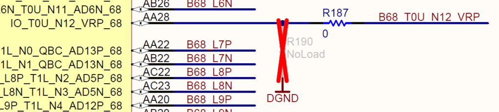
VRP Pins
The XEM8370 routes the multi-purpose VRP pins to the expansion connectors. To support certain IOSTANDARD‘s like MIPI you can remove the 0Ω resistor jumper connecting these pins to the expansion connector, and insert a 240Ω resistor at the available location to pull the pin to ground.
Please see the UltraScale Architecture SelectIO Resources for more details about the VRP pin and IOSTANDARD support.
| VRP Pin | FPGA PIN | Expansion COnnector 0Ω Jumper | Ground Resistor |
|---|---|---|---|
| B64_T0U_N12_VRP | AP19 | R192 | R194 |
| B66_T0U_N12_VRP | A8 | R193 | R195 |
| B67_T0U_N12_VRP | AD24 | R186 | R189 |
| B68_T0U_N12_VRP | AA28 | R187 | R190 |
| B69_T0U_N12_VRP | AC29 | R188 | R191 |
VBATT
VBATT is by default connected to ground via R91. It is also connected to MC2 pin 13. For information on using VBATT for encryption key storage see the Encryption Key Storage page.
SmartVIO I2C
The expansion connector MC2 has pins used for I2C communication with SYZYGY devices. If SYZYGY ports are placed on a carrier board they must be connected to these pins to implement SmartVIO. See the Device Settings page for more details. The BRK8370 is an example of this implementation.
I/O State at Power On
AMD Kintex UltraScale+ FPGAs support a weak pull-up state on all I/O pins from power on until first configuration. This behavior is controlled by the PUDC_B pin. By default the XEM8370 holds the PUDC_B pin high with a 1kΩ resistor at R38, disabling the weak pull-up on all I/O pins at power on. This behavior can be changed by inserting a 0Ω resistor at R41 and removing the 1kΩ resistor at R38, forcing the PUDC_B pin low.