Specifications
| Host Interface | USB 3.0 Type C, SuperSpeed FrontPanel Support |
| FPGA | XCKU11P-1FFVA1156E XCKU11P-3FFVA1156E (optional) |
| Memory | 4 GiByte DDR4, 32-bit wide data interface |
| NV Memory | 16 MiB System Flash 32 MiB FPGA Flash |
| Clocks | 100 MHz fixed fabric oscillator 6 pin 2.5×2.0mm or 2.5×3.2mm footprint RefClock options available RefClock inputs on Expansion Connectors |
| FPGA I/O | 253 HP I/O (Banks 64, 66, 67, 68, 69) 48 HD I/O (Banks 88, 89) |
| FPGA MGT | 20 GTH transceivers (12.5 Gb/s) 8 GTY transceivers (16.3 Gb/s) |
| Dimensions | 120 x 85mm (4.72 x 3.35″) |
| MINIMUM | TYPICAL | MAXIMUM | UNITS | |
|---|---|---|---|---|
| DC Input | +5.0 | – | +18.0 | VDC |
| DC Input Ripple | – | – | 50 | mVp-p |
| Operating Temperature | 0 | – | +70 | ºC |
| Storage Temperature | -50 | 0 | +100 | ºC |
| Weight | 91.5 | grams | ||
| Oscillator Frequency (Fixed Fabric) | 100 | MHz | ||
| Oscillator Period Jitter | 2.5 | psRMS | ||
| Oscillator Stability | ±25 | ppm |
| KU11p | |
|---|---|
| System Logic Cells | 653,100 |
| CLB Flip-Flops | 597,120 |
| CLB LUTs | 298,560 |
| Max. Distributed RAM (Mb) | 9.1 |
| Block RAM | 600 blocks (21.1 Mb) |
| UltraRAM | 80 blocks (22.5 Mb) |
| DSP Slices | 2,928 |
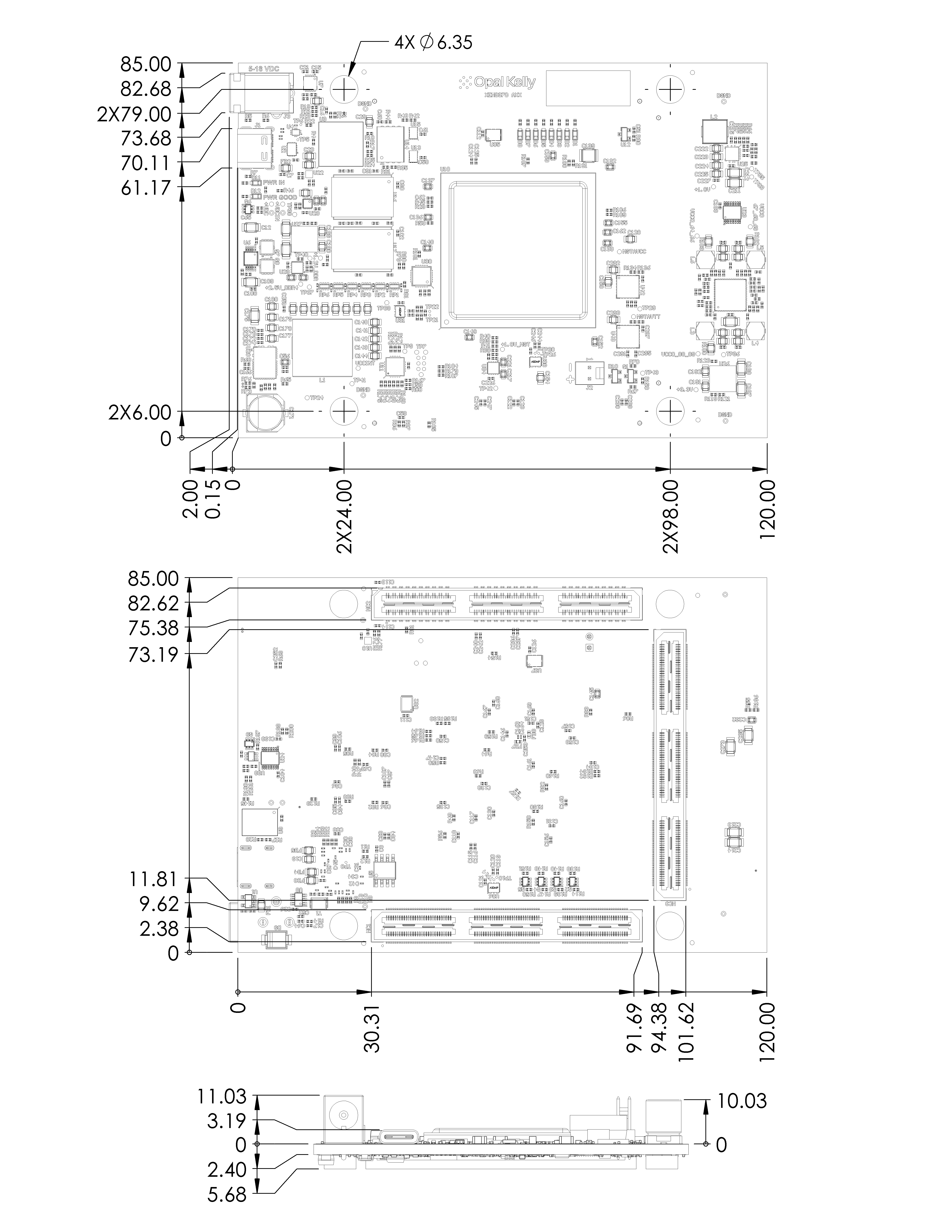
PCB Footprint
The PCB is 120 x 85mm (4.72 x 3.35″) with four mounting holes spaced as shown in the drawings below. The mounting holes accept Samtec JSO jack standoffs for controlled mating and unmating with a carrier board. The JSO mounting holes are unplated. The two board edge connectors (USBC and DC power) overhang the PCB slightly in order to accommodate mounting within an enclosure.
The XEM8350 has three high-density 0.5mm connectors providing access to 301 I/O, 28 multi-gigabit transceivers, and multiple electrically-programmable adjustable voltages.
Mechanical Drawing
The mechanical drawing below may be used for enclosure or mounting hardware design. 3D Models are also available in SolidWorks, STEP, and IGES formats.
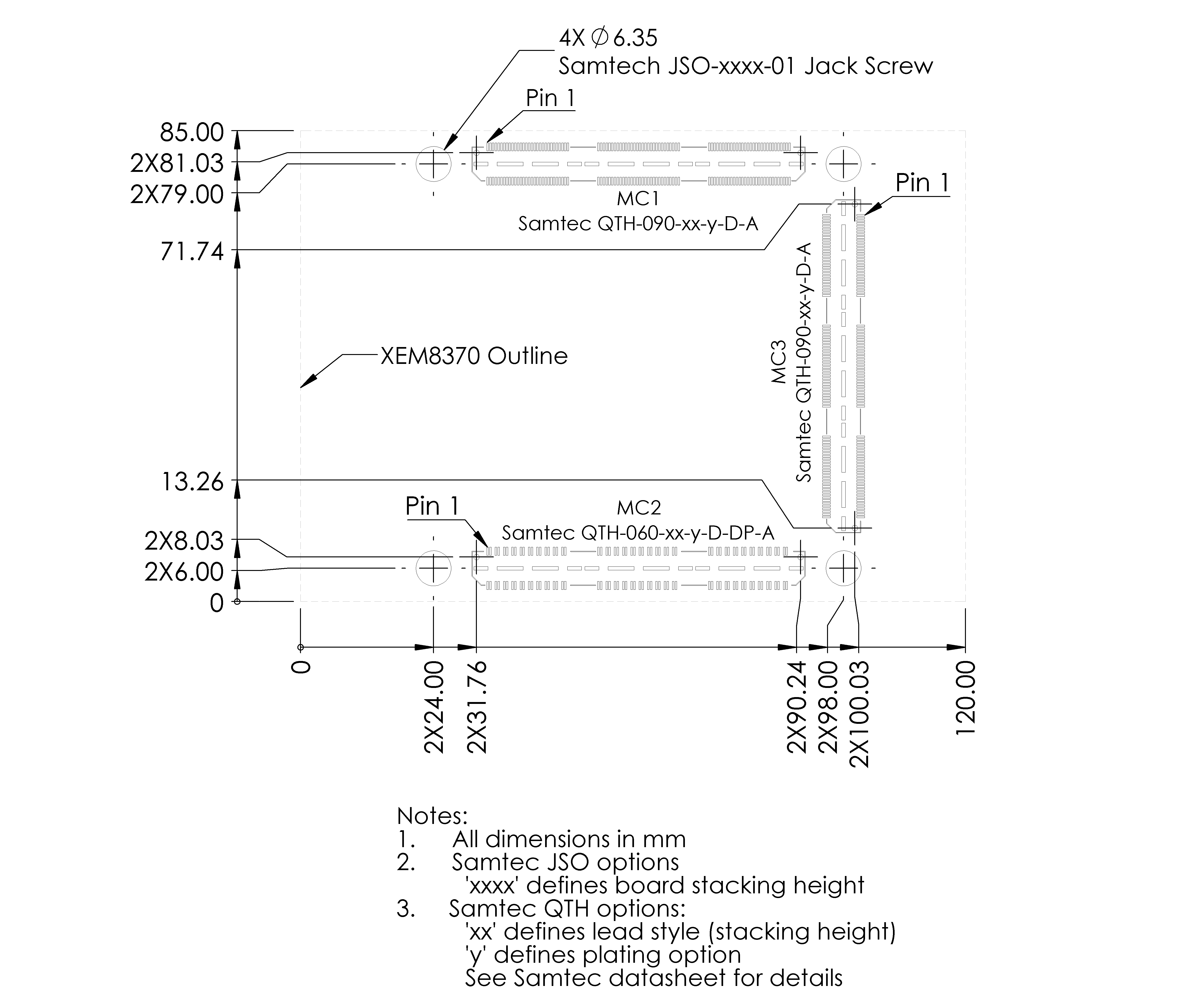
Mating Board Diagram
Use the mating diagram below to orient and design peripheral mating hardware. Note that this is a top-down view and mates to the bottom of the XEM8370. This design is realized in Altium CAD drawings in the corresponding breakout board which are available through Pins Downloads.
For Samtec connector details, drawings, models, and landing patterns, please visit Samtec’s website.