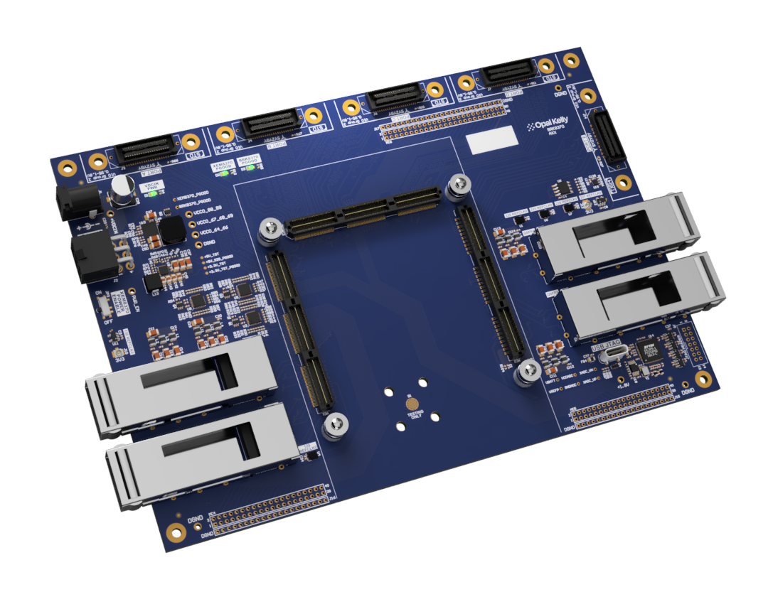
BRK8370 Breakout Board
Powering the BRK8370
The BRK8370 requires a clean, filtered, DC supply within the range of 6 V to 18 V. This supply may be delivered in one of two ways:
- 6-pin Mini-Fin connector – Pins 1, 2, and 3 are tied to the input supply net +VDCIN. Pins 4, 5, and 6 are tied to ground. The total maximum current allowed over this connector is 8 A. The part number is Molex 0455580003. The mating plug part number is Molex 0455590002. Several options for crimping pins are available, including Molex 0039000038. While it is possible to provide power using a commercial PC power supply with compatible pinout, it is recommended to create a custom cable harness for use with an appropriate bench supply.
- DC barrel jack – The jack is part number PJ-102AH from CUI, Inc. It is a standard “canon-style” 2.1mm / 5.5mm jack. The outer ring is connected to DGND. The center pin is connected to +VDCIN.
Please refer to Powering the XEM8370 for information on the XEM8370 power systems.
Regulators on the BRK8370 provide 3.3V and 5V power for the onboard SYZYGY and QSFP+ ports.
| Power Rail | Supply Capacity | Uses |
|---|---|---|
| +3.3V_TST | 7A | QSFP and SYZYGY 3.3V |
| +5V_TST | 4.5A | SYZYGY 5V |
LED Indicators
The BRK8370 includes three LED indicators for power status. The XEM8370_PGOOD and BRK8370_PGOOD signals are also broken out to test points. These are 3.3V, good when high signals.
| LED | ON CONDITION |
|---|---|
| VDCIN PWR (D1) | +VDCIN present |
| XEM8370 PGOOD (D2) | All XEM8370 on-board power supplies active and within expected range (Does not include VIOx supplies) |
| BRK8370 PGOOD (D3) | All BRK8370 on-board power supplies active and within expected range |
IPMI EEPROM
The XEM8370 may optionally read peripheral information and configuration data from a small EEPROM on the peripheral. If available, the EEPROM can be used to automatically set the voltages for the three programmable voltage regulators on the XEM8370. An EEPROM is installed on the BRK8370 but is not loaded with any configuration by default.
See the Expansion Connectors page Peripheral Personality EEPROM section for more information.
Peripherals and Connectors
The XEM8370 Pin List has full connection information in the “BRK8370” columns. Additionally, please refer to the schematics and layout available on the Pins downloads page for detailed connection diagrams.
SYZYGY Ports
For information on the SYZYGY ports see the BRK8370 SYZYGY Ports page.
QSFP+ Transceiver Sockets
The BRK8370 has four QSFP+ cages installed. Full QSFP transceiver connection pinout and control signal I/O connections are listed on the XEM8370 Pin List.
| CONNECTOR TYPE | REFDES | MGT | Control Signal I/O |
|---|---|---|---|
| QSFP1 | J8 | GTY 130 | Bank 68 |
| QSFP2 | J9 | GTY 129 | Bank 68 and 69 |
| QSFP3 | J30 | GTH 228 | Bank 69 |
| QSFP4 | J31 | GTH 227 | Bank 68 and 69 |
QSFP transceivers are not included. The following 10Gtek part is one example option.
| MANUFACTURER | PART NUMBER | DESCRIPTION | APPROXIMATE COST |
|---|---|---|---|
| 10Gtek | AMQ10-SR4-M1 | 40GBASE-SR4 QSFP+ Transceiver for MMF, 100M | $39.00 / each |
2mm I/O Headers
The rest of the unused I/O are broken out into 3 banks of 2mm headers. Each header bank also has a row of ground pins. The headers pins are unpopulated by default.
The I/O voltage level of different banks can be controlled with the adjustable voltage regulators on the XEM8370. See the Device Settings page for more details.
For full I/O connection details see the XEM8370 Pin List.
| Header Designator | Pin Count | Connected Banks | Other |
|---|---|---|---|
| MC4 | 40 I/O | 68 and 69 | |
| MC5 | 38 I/O | 64, 68 and 69 | VCCO_64_66 and VCCO_67_68_69 |
| MC6 | 48 I/O | 88 and 89 | VCCO_88_89 |
JTAG
The BRK8370 has a built in USB JTAG adapter. Connect to the USB-C connector J11 for AMD tools compatible access to the XEM8370’s JTAG interface.
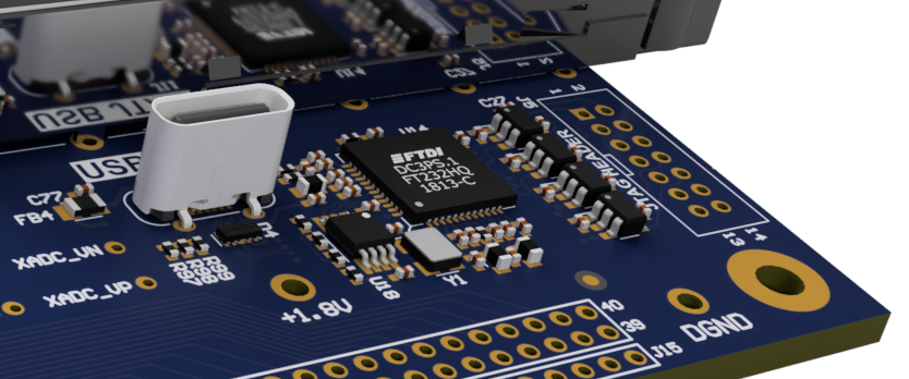
The JTAG connections are also wired to a dedicated 2mm header J5 that can be used with a compatible JTAG cable. The JTAG interface presented is at a 1.8V signaling voltage. This header is not populated by default. This footprint is compatible with the Molex part 87831-1420.
| CONNECTOR PIN | JTAG SIGNAL | CONNECTOR PIN | JTAG SIGNAL |
|---|---|---|---|
| 1 | GND | 2 | +1.8V (Vref) |
| 3 | GND | 4 | JTAG_TMS |
| 5 | GND | 6 | JTAG_TCK |
| 7 | GND | 8 | JTAG_TDO |
| 9 | GND | 10 | JTAG_TDI |
| 11 | GND | 12 | NC |
| 13 | GND | 14 | NC |
Clock Oscillator
There are two clock oscillators onboard the BRK8370. These supply 156.25Mhz clocks to both the GTY and GTH banks, which supports a wide variety of Ethernet protocol options to use with the QSFP ports.
Additionally there are two open 3.2 x 2.5mm 6 pin LVDS oscillator footprints available on the BRK8370 to allow for additional clock frequencies to be added if required. These footprints are compatible with oscillators like the SIT9120AI-2B3-XXE156.250000.
| CLOCK | DEsignator | FREQUENCY | MC PINS | FPGA PINS (P / N) | Note |
|---|---|---|---|---|---|
| MGT 129 REFCLK0 | U4 | 156.25 Mhz | MC1 26 / 28 | R29 / R30 | |
| MGT 226 REFCLK0 | U10 | 156.25 MHz | MC2 66 / 68 | V6 / V5 | |
| MGT 225 REFCLK0 | U6 | — | MC2 65 / 67 | AB6 / AB5 | Not Placed |
| MGT 228 REFCLK0 | U7 | — | MC2 46 / 48 | K6 / K5 | Not Placed |
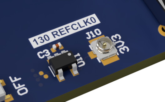
MGT External Refclock Inputs
Two external refclock inputs are available on the BRK8370. These allow for a 3.3V LVCMOS external clock to be connected to the provided U.FL connector. The clock will be converted to LVDS on board and fed into the associated XEM8370 refclock. Details on these connections are listed in the table below.
| CLOCK | Connector DESIGNATOR | MC PINS | FPGA PINS (P / N) |
|---|---|---|---|
| MGT 130 REFCLK0 | J10 | MC1 25 / 27 | L29 / L30 |
| MGT 227 REFCLK0 | J12 | MC2 45 / 47 | P6 / P5 |
Power Enable Switch
The XEM8370 has a pin on the expansion connector that can control the main power to the board. When this pin is not connected, the board will power on normally. If the pin tied to ground, the VDCIN protection circuit will remain disabled and keep the board powered off. The XEM8370 POWER ENABLE switch on the BRK8370 allows you to pull this pin to ground if desired.
Additionally this PWR_EN signal is brought out to a test point next to the switch.
FPGA ADC
The FPGA’s ADC related pins are brought out to test points on the BRK8370. See the Expansion Connectors page for more information.
XEM8370 Mounting
The XEM8370 uses multiple high pin count expansion connectors. Care must be taken when mounting and unmounting from the BRK8370. See the Jack Screw Instructions page for the proper mounting procedure.
Schematic and Design Files
The BRK8370 schematics and design files are available in the Downloads section of the Pins website.
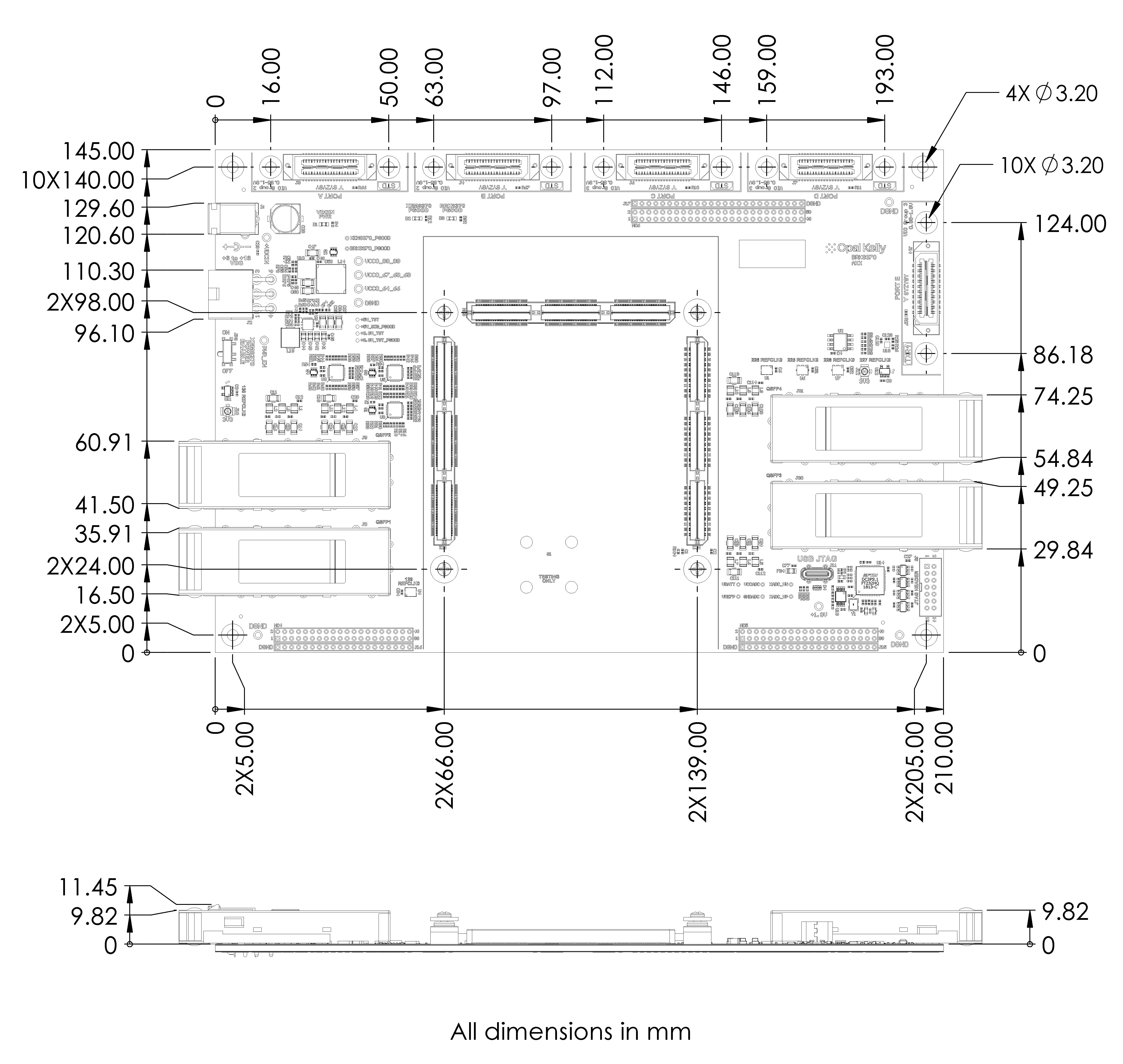
Mechanical Drawing
3D Models are available in SolidWorks, STEP, EASM and IGES formats.
Rev AXX