Powering the XEM8370
The XEM8370 requires a clean, filtered, DC supply within the range of 5 V to 18 V. This supply may be delivered through the DC power connector (rated to 5 A max current) or through the expansion connectors (rated to 16 A max current).
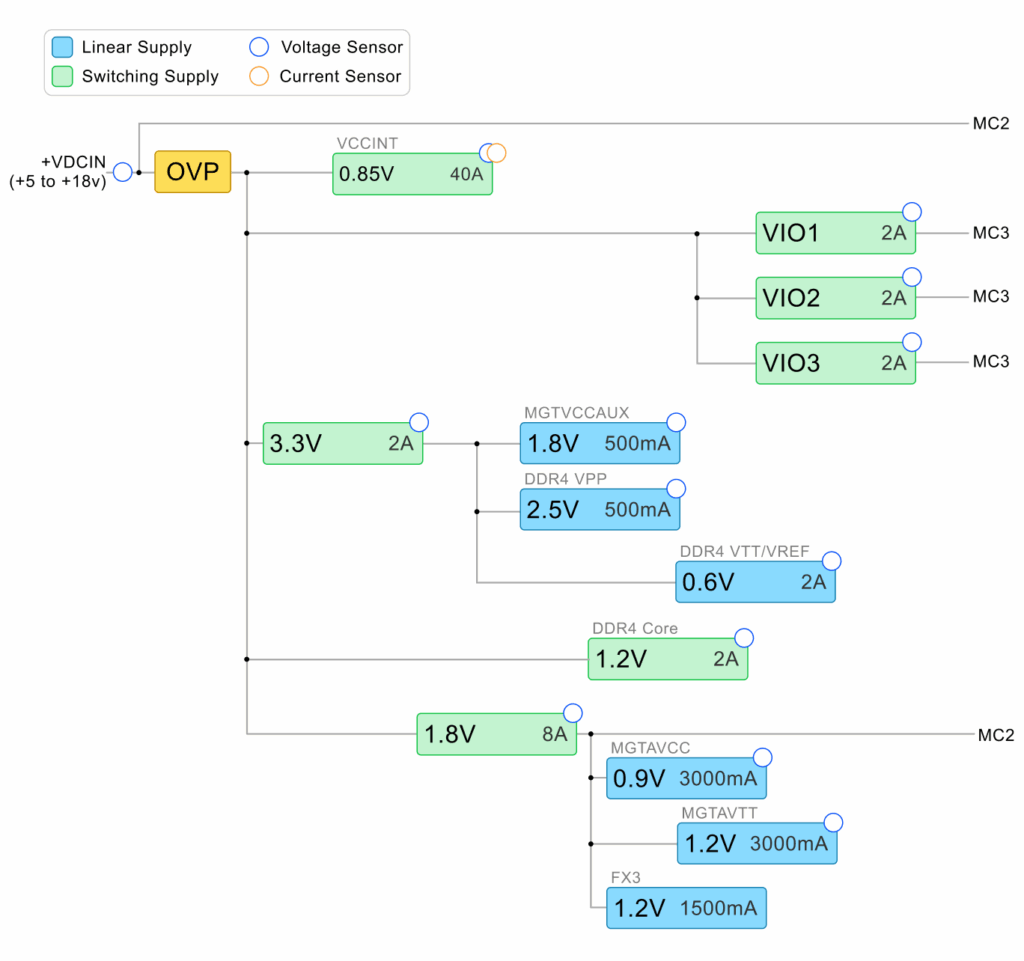
The XEM8370 power distribution system is quite complex, with several supplies designed to provide suitable, efficient power for several systems and modules. A block diagram of the system follows, with input (+VDC) shown to the left and accessible supply rails shown to the right.
Power Supply
The XEM8370 is designed to be operated from a single 5-18 V power source supplied through a DC power connector on the device. This provides power for the several high-efficiency switching regulators on-board to provide multiple DC voltages for various components on the device as well as three adjustable supplies for the I/O levels. Status monitoring for many of these rails is available in the Device Sensors.
Barrel Jack Power Connector
The barrel jack power connector on the XEM8370 is part number PJ-102AH from CUI, Inc. It is a standard “canon-style” 2.1mm / 5.5mm jack. The outer ring is connected to DGND. The center pin is connected to +VDC. The PJ-102AH jack is rated for 5 A maximum continuous current.
Expansion Connector Power
Input power be supplied to the board through the expansion connector. In total the expansion connector can carry 16A for VDCIN. See the VDCIN pin connections in the Pins sheet.
Over-Voltage Protection and Under-Voltage Lockout
The XEM8370 includes an over-voltage protection circuit which disconnects the input supply from the on-board circuitry when the input is higher than approximately 18.4 V. It is also prevented from powering on when the input supply is below approximately 4.5V. And it is protected from reverse polarity voltage connected to the input.
Bank I/O Power
The XEM8370 includes 3 on board adjustable regulators that power different I/O bank rails. The available I/O are distributed across these rails to allow for connections to multiple voltage domains. For more information on configuring the adjustable voltage regulators see the Device Settings page.
| VIO | I/O BANK | VCCO RAil |
|---|---|---|
| VIO1 | 88 and 89 | VCCO_88_89 |
| VIO2 | 67, 68 and 69 | VCCO_67_68_69 |
| VIO3 | 64 and 66 | VCCO_64_66 |
LED Indicators
The XEM8370 includes two LED indicators for power status.
| LED | ON CONDITION |
|---|---|
| PWR IN (D11) | +VDCIN present, no over-voltage or reverse voltage faults |
| PWR GOOD (D12) | All on-board power supplies active and within expected range (Does not include VIOx supplies) |
Power Budget
The table below can help you determine your power budget for each supply rail on the XEM8370. All values are highly dependent on the application, speed, usage, and so on. Entries we have made are based on typical values presented in component datasheets or approximations based on AMD power estimator results. Shaded boxes represent unconnected rails to a particular component. Empty boxes represent data that the user must provide based on power estimates.
The user may also need to adjust parameters we have already estimated (such as FPGA Vcco values) where appropriate. All values are shown in milliwatts (mW). Note that this table does not include the two supplies dedicated to the GTH transceivers. These are independent and can be computed separately for power budget based on their assigned function.
| COMPONENT(S) | 0.85 V | 0.9 V | 1.2 V | 1.2 V | 1.8 V | 3.3 V | VIO1 | VIO2 | VIO3 |
|---|---|---|---|---|---|---|---|---|---|
| Fabric Oscillator | 55 | ||||||||
| FX3 USB Host Interface | 490 | ||||||||
| DDR4 VDD/VDDQ | 630 | ||||||||
| DDR4 VTT Termination | 460 | ||||||||
| DDR VPP | 100 | ||||||||
| FPGA VCCINT, VCCINT_IO, VCCBRAM | |||||||||
| FPGA MGTAVCC | 1350 | ||||||||
| FPGA MGTAVTT | 3170 | ||||||||
| FPGA MGTVCCAUX | 110 | ||||||||
| FPGA VCCAUX, VCCAUX_IO | 965 | ||||||||
| FPGA VCCO65 (USB Host Interface) | 25 | ||||||||
| FPGA VCCO70 + VCCO71 (1.2V DDR4) | 230 | ||||||||
| FPGA VCCO88 + VCCO89 (VIO1) | |||||||||
| FPGA VCCO67 + VCCO68 + VCCO69 (VIO2) | |||||||||
| FPGA VCCO64 + VCCO66 (VIO3) | |||||||||
| Total (mW) | 1350 | 3170 | 1320 | 1645 | 100 | ||||
| Available (mW) | 34,000 | 2,700 | 3,600 | 2,400 | 14,400 | 6,600 | 2000 mA 1.2-3.3V | 2000 mA 0.95-1.8V | 2000 mA 0.95-1.8V |
Example XEM8370-KU11P FPGA Power Consumption
AMD XPower Estimator 2020.1.1 was used to compute the following power estimates for the Vccint supply. These are simply estimates; your design requirements may vary considerably. The numbers below indicate approximately 80% utilization.
| COMPONENT | PARAMETERS | VCCINT POWER (MW) |
|---|---|---|
| Clock | 200 MHz GCLK, 400,000 fanout | 1,132 |
| Clock | 300 MHz GCLK, 140,000 fanout | 954 |
| Clock | 200 MHz SR, 50,000 fanout | 258 |
| Logic | 200 MHz, 90,000 logic LUTs, 50,000 shift registers, 50,000 distributed RAMs, 350,000 registers | 3,367 |
| Logic | 300 MHz, 50,000 logic LUTs, 140,000 registers | 1509 |
| Logic | 1200 MHz (DDR4), 8000 logic LUTs | 383 |
| BRAM | 18-bit, 200 MHz, 500 block RAMs, 12.5% toggle rate | 228 |
| BRAM | 36-bit, 200 MHz, 250 block RAMs, 12.5% toggle rate | 226 |
| DSP | 200 MHz, 2500 slices, 12.5% toggle rate | 2,299 |
| GTH | 20 channels, 12.5 Gb/s | 767 |
| GTY | 8 channels, 16.375 Gb/s | 425 |
| Misc. | DCM, PLL, VCCINT_IO, etc. | 500 |
| Total | 12,048 mW | |
| Available | 38,000 mW |