Pins
Opal Kelly Pins is an interactive online reference for the expansion connectors on all Opal Kelly FPGA integration modules. It provides additional information on pin capabilities, pin characteristics, and PCB routing. Additionally, Pins provides a tool for generating constraint files for place and route tools.
We have tried to capture significant FPGA pin capabilities in the Pin List. However, the FPGA Datasheet should be used as the authority on pin capabilities and design considerations.
Toolbar
The toolbar at the top of a Pins product page has a number of features. Explore a bit; you won’t break it.

Search
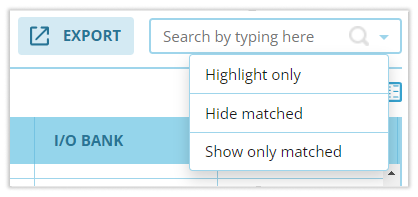
You can search the pin list using the search entry at the top-right. Click on the magnifying glass drop-down to adjust the function of the search to one of:
- Highlight – Highlights search results only.
- Hide Matching – Hides rows where search matches are found.
- Show Only Matching – Shows only rows where a search match is found.
Exporting a Pin List or Constraints File
Use the Export button on the toolbar to export the pins list.
Select Export as CSV to save a CSV version of the Pin List which can be loaded into a spreadsheet for further manipulation offline. All columns, including filterable columns which are not necessarily displayed in the Pin List are exported to the CSV.
Select Export as PDF to generate a PDF containing the filtered Pin List for printing.
Select Generate Constraints File to generate a template XDC/UCF file for the device. The constraints file will contain a comprehensive list of all expansion connector FPGA pins and all additional device features.
Pin Lists
As the primary reference for Opal Kelly integration module expansion connectors, Pin Lists contain a comprehensive table of the FPGA-to-Connector data including connector pin, FPGA pin, signal description, routed length (when applicable), breakout board pin mapping, FPGA I/O bank, and other properties.
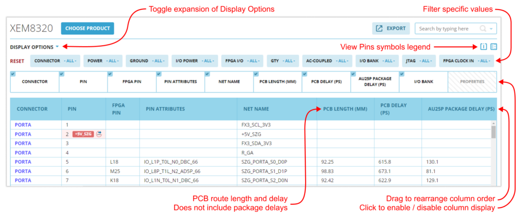
Table Customization
A number of customizations are available by expanding the DISPLAY OPTIONS panel at the top of the Pin List. The available table columns may be reordered by dragging their respective tab to a new location or individually enabled / disabled by clicking on the tab.
Note that we have designated some of the available columns as disabled by default to focus attention on the most commonly used information.
Filters
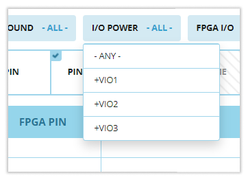
Each pin list has several properties defined for each pin. The Display Options panel has a list of these properties which can be used to filter displayed pins for easier navigation and project definition. When a specific attribute value is selected, Pins will display only those device pins that match the attribute value.
Filters can be used to quickly identify groups of pins that fit a particular purpose. For example, most Pin Lists have a boolean property called FPGA I/O that is set to true for any connector pin that is routed to an available I/O on the FPGA. Filtering on this property removes all expansion pins that are not I/Os, allowing you to focus on available connections for your design.
View Density
Near the pins symbols legend button in the top right is a Table Layout button that toggles the table cell density between two settings.
Presentation
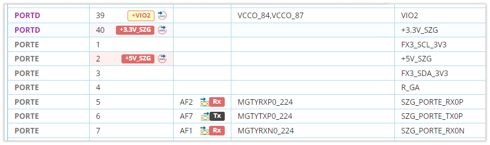
Each product’s Pin List is presented in table form with one row representing a single pin on one of the expansion connectors. The cells within the row contain various information associated with that pin such as connector reference designator, pin number, the FPGA location routed to the pin, routed length, and other attributes. A number of standard symbols are used to represent qualities of a pin such as the presence of ac-coupling, the I/O functionality of the pin, or power connections. A legend describing these symbols is available by clicking an icon at the top right of the Pin List.
Column Details
| COLUMN NAME | DESCRIPTION |
|---|---|
| Connector | The expansion connector designator. |
| Pin | The expansion connector pin number. |
| FPGA Pin | The FPGA pin the net is connected to. |
| Pin Attributes | The full FPGA pin name. A number of special information is conveyed in this name, such as Global Clock and ADC pins. This is a quick reference all of the functions the pin provides. |
| Net Name | The signal net name on the product. |
| PCB Length (MM) | The route length between the FPGA and the Expansion Connector. This length does not include the package delay on the FPGA. |
| PCB Delay (pS) | The route delay between the FPGA and the Expansion Connector. This delay does not include the package delay on the FPGA. |
| Package Delay (pS) | The pin/package delay provided by the FPGA manufacturer for the specific FPGA version. |
| I/O Bank | The FPGA bank used for the I/O. |
| BRK | The break out board pin connection for the I/O signal. |
Pin Diagrams
Pin Diagrams can help you identify the location of pins on the module. To open the pin diagram for a Pin List, click on any of the rows in the list. The diagram will appear in a section at the top of the page. As you hover over pin list table rows, the corresponding pin in the diagram will highlight.
Peripherals
A Peripheral is a user-defined set of signal names that associate to the pins on a pin list. Peripherals help you define the expansion pinout for your attached device and HDL design. Pins can automatically generate the constraint file used in AMD and Intel place and route tools based on the Pins source data and your peripheral.
You will need to be logged in as your Pins user to create new peripherals. After logging in Peripherals will be available in the left sidebar.
Creating a New Peripheral
Create a new Peripheral by clicking New Peripheral on the Peripherals List, then select a Pin List that will define the Peripheral and add a name and description to identify the Peripheral. After you’ve created the Peripheral, you’ll be able to define more details about how constraints files will be generated.
Design Entries
Each Pin List has at least one column that may be used to specify additional information for some pins. For example, the column Design Net represents the name of a signal net within your FPGA HDL design that is associated to an external pin. This is required for FPGA pin location mapping within the constraint file. These user columns are not visible on the Pin List, but they contain editable fields that are stored with the Peripheral and exported to the Constraint File as needed.
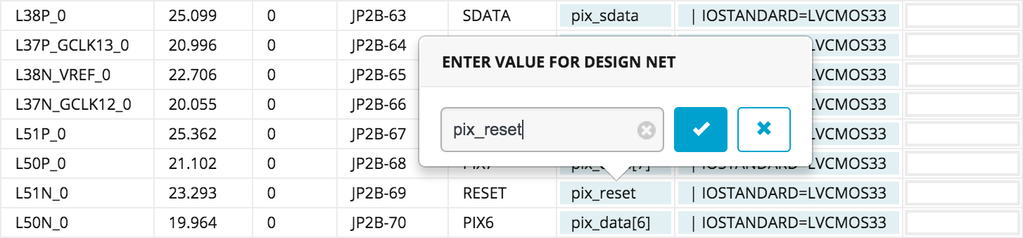
Specifying Net Names
The Pin List view for a Peripheral includes three additional, editable columns:
- Design Net – The name of the signal as it appears in your top-level HDL.
- Constraints – Text that is inserted into the constraints file for that signal.
- Comment – Additional comment text that is added to the constraints file.
These additional data are merged with the default Pin List constraints file prior to export. The result is a constraints file complete with net names that can be used with your FPGA development flow.
Constraint File Generation (XDC / UCF / QSF)
One of the primary motivations for the Peripherals feature is the automatic generation of AMD and Altera constraint files, known as XDC, UCF (AMD), or QSF (Altera) files. These files are used by the place and route tools to assign signal nets to particular pin locations on the FPGA package. Correspondingly, they are how signal nets get mapped to specific pins on the integration module. Automating this process through Pins greatly simplifies the process of mapping the signals in your HDL to pins on the module.
Click on the Export button and select Generate Constraints File from the Peripheral Editor (or the Peripheral List) at any time to generate the constraint file.
Selecting Module Features
In addition to the expansion connections, Opal Kelly FPGA integration modules contain other features such as pushbuttons, LEDs, memory, and the FrontPanel host interface. Depending on your application, you may want to include the constraints for one or more of these additional features in your constraints file. You can enable or disable each feature in the Peripheral Details by clicking on the peripheral name at the top of the Peripheral Editor.
In addition to the standard features, we’ve provided user-definable Lead In and Lead Out sections.
