SZG-QSFP
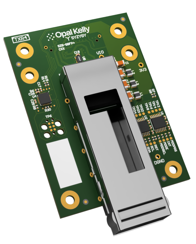
The SZG-QSFP is a SYZYGY Transceiver (TXR4) peripheral with one cage for an appropriate QSFP+ module.
Resources
- Aligni PLM – See the Attachments tab for schematics.
- SYZYGY Specification
- SYZYGY GitHub Site – Several projects that could be helpful.
- Product Page
Design
The SZG-QSFP allows connecting a QSFP+ module to an FPGA transceiver bank via the SYZYGY TXR4 port. All of the QSFP+ module control signals are connected to IO and have level shifting on board to allow for a variety of compatible bank voltages.
Primary Components
| COMPONENT | MANUFACTURER | MANUFACTURER P/N |
|---|---|---|
| QSFP Cage | Amphenol | U95-T111-1001 |
| QSFP+ Receptacle | Amphenol | FS1-Z38-20Z6-60 |
Reference Clock
An on board 156.25Mhz oscillator is provided as a transceiver reference clock. This frequency is compatible with a variety of Ethernet protocols.
| SYZYGY Port Pin | Signal Name |
|---|---|
| 13 | REFCLKp |
| 15 | REFCLKn |
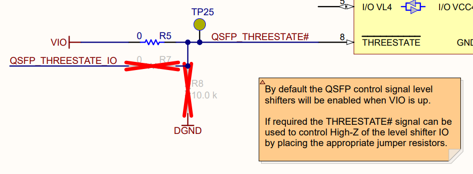
Control I/O Tri-State
Normally the QSFP control signals are tri-stated (high impedance) whenever either 3.3V or VIO is down. However this function can be manually controlled via an I/O pin, if required. To do so remove R5 and place R7 and R8.
| SYZYGY PORT PIN | SIGNAL NAME | Schematic Net |
|---|---|---|
| 22 | S7 | QSFP_THREESTATE_IO |
SYZYGY Information
Compatibility Table
| COMPATIBILITY PARAMETER | SPECIFICATION |
|---|---|
| Port type | SYZYGY Transceiver (TXR4) |
| Width | Single |
| 5V supply required | No |
| Nominal 5V supply current | N/A |
| Nominal 3.3V supply current | 1000mA |
| VIO supply voltage | 1.2V – 3.3V |
| Nominal VIO supply current | 10mA |
| Total number of I/O | 8 |
DNA Data
| DNA PARAMETER | DATA |
|---|---|
| Max 5V Load | 0mA |
| Max 3.3V Load | 1500mA |
| Max VIO Load | 10mA |
| IS_LVDS | False |
| IS_DOUBLEWIDE | False |
| IS_TXR4 | True |
| VIO Range(s) | [1.2,3.3] |
Pinout
See the SZG-QSFP schematic for more information.
- Column
PIN NUM (J1)lists the pin number on the SYZYGY specification’s Standard Samtec connector, this is reference designator J1 in the schematic. - Column
SIGNAL NAMElists the SYZYGY specification’s name for this pin’s connection. - Column
SCHEMATIC NETlists the net name found in the SZG-QSFP’s schematic for the connection.
| PIN NUM (J1) | SIGNAL NAME | SCHEMATIC NET | Note |
|---|---|---|---|
| 5 | RX0p | QSFP_RX1P | |
| 6 | TX0p | QSFP_TX1P | |
| 7 | RX0n | QSFP_RX1N | |
| 8 | TX0n | QSFP_TX1N | |
| 9 | RX1p | QSFP_RX2P | |
| 10 | TX1p | QSFP_TX2P | |
| 11 | RX1n | QSFP_RX2N | |
| 12 | TX1n | QSFP_TX2N | |
| 13 | REFCLKp | REFCLKP_C | 156.25Mhz LVDS Clock |
| 14 | S0 | QSFP_MODPRS_B_VIO | |
| 15 | REFCLKn | REFCLKN_C | 156.25Mhz LVDS Clock |
| 16 | S1 | QSFP_INT_B_VIO | |
| 17 | S2 | QSFP_LP_MODE_VIO | |
| 18 | S3 | QSFP_SCL_VIO | |
| 19 | S4 | QSFP_MODSEL_B_VIO | |
| 20 | S5 | QSFP_SDA_VIO | |
| 21 | S6 | QSFP_RESET_B_VIO | |
| 22 | S7 | QSFP_THREESTATE_IO | |
| 25 | RX3p | QSFP_RX4P | |
| 26 | TX3p | QSFP_TX4P | |
| 27 | RX3n | QSFP_RX4N | |
| 28 | TX3n | QSFP_TX4N | |
| 29 | RX2p | QSFP_RX3P | |
| 30 | TX2p | QSFP_TX3P | |
| 31 | RX2n | QSFP_RX3N | |
| 32 | TX2n | QSFP_TX3N |