PCI Express Reference Design
By the end of this tutorial you will have successfully used the BRK8310 with an XEM8310 to initiate DMA transfers between the BRK8310+XEM8310 gateware and the host PC. The steps will guide you through the process of generating the gateware, configuring your host system, bringing up your hardware, and successfully running the test procedure to validate your system.
This tutorial utilizes AMD’s DMA/Bridge Subsystem for PCI Express IP’s example design along with AMD’s provided example drivers. This tutorial uses the Ubuntu operating system, but Windows 10 drivers are also available.
Requirements:
Resources
- AMD PCI Express DMA Drivers and Software Guide for Linux and Windows (AR65444)
- DMA Subsystem for PCI Express (Product Page)
- XDMA GitHub repository Linux driver and application sources.
- Pins Reference
Top-Level Architecture
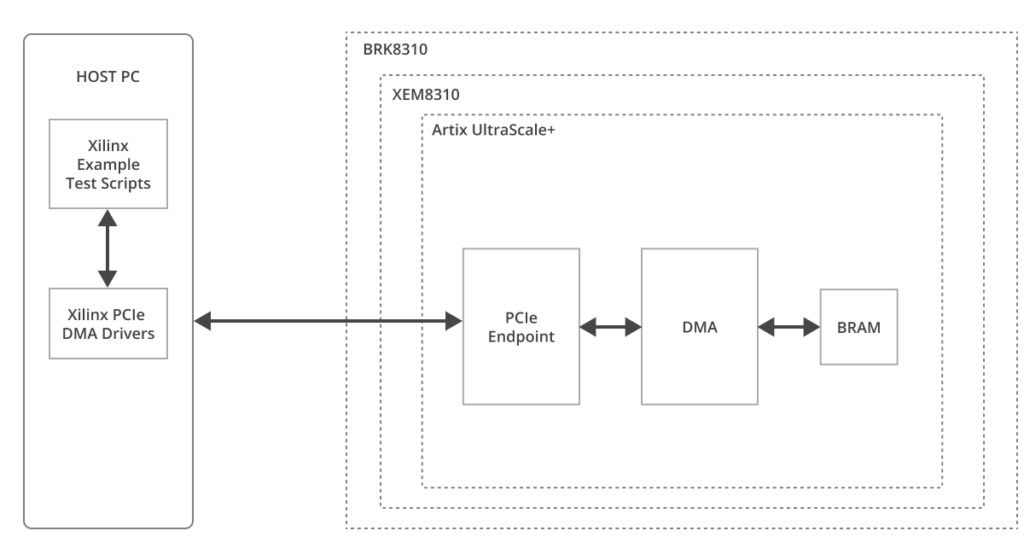
The DMA/Bridge Subsystem for PCI Express IP’s example design is generated by Vivado. The example design implements a 4KByte BRAM buffer that is read or written to via DMA. AMD’s provided drivers/applications initiate the DMA transfers to and from the BRAM on the XEM8310.
Tutorial
We provide two tutorials that result in different power-on procedures:
- Standard – The BRK8310 and host PC are powered separately. The system is powered and programmed in a manual sequence that ensures a proper enumeration. This method is less complicated and allows more flexibility for the implemented design.
- Tandem – The BRK8310 and host PC are powered using the host PC’s PSU and the PCIe device enumerates when the PC is powered on. The bitfile is split into two stages. The first stage includes just the PCIe components that enumerate the PCIe device, the second stage includes the rest of the implemented design. This segmented bit file is loaded into the FPGA flash onboard the XEM8310 and configures the FPGA at power-on. The smaller first stage ensures that the PCIe device is available to the host PC in under 100ms (PCIe specification), allowing a successful enumeration. This method is more complicated and comes with some caveats for the implemented design.
Standard Configuration
Create a New Vivado Project
- Open a New Vivado project.
- Select the
xcau25p-ffvb676-2-eFPGA part. - Configure the DMA/Bridge Subsystem for PCI Express IP from the IP wizard.
- Select a lane width of x8.
- Select the maximum link speed available through the GUI.
- All other settings can be kept at their default. Press “OK” to create the IP.
- Right click on the IP in the hierarchy view and select “Open IP Example Design”.
Make Board-Specific HDL Modifications
1. Open up the example design’s xilinx_xdma_pcie_x0y0.xdc constraint file.
2. Remove the LOC constraints for ports sys_rst_n, sys_clk_p, and sys_clk_n. Substitute them with the following constraints. Package pin information can be obtained from the XEM8310’s Pins page.
set_property PACKAGE_PIN E22 [get_ports sys_rst_n]
set_property PACKAGE_PIN T7 [get_ports sys_clk_p]
set_property PACKAGE_PIN T6 [get_ports sys_clk_n]Code language: CSS (css)
3. Generate the bitstream.
Power-on Procedure
The PCIe device must be powered and available at the time the host PC enumerates the PCIe bus at power-on. Follow the following procedure to configure your hardware correctly:
- Power-off your host PC.
- Plug in the BRK8310 into a compatible PCIe port.
- Power-on your XEM8310 using the barrel jack power connector. See Power Connectors.
- Program the PCIe DMA bitfile into your XEM8310.
- Power-on your host PC.
Confirm Enumeration
- Run
sudo lspci -vvvto see verbose information about the devices enumerated onto the PCIe bus of the host PC. The device will be enumerated under the name “Xilinx Corporation Device”.
Install Drivers
- Acquire the sources at the following Git repository: XMA
- Follow the README’s instructions for installation.
Run the Tests
- Run the following AMD provided tests from the XMA Git repository:
run_tests.shperform_hwcount.sh
Tandem Configuration
Create a New Vivado Project
- Open a New Vivado project.
- Select the
xcau25p-ffvb676-2-eFPGA part. - Configure the DMA/Bridge Subsystem for PCI Express IP from the IP wizard.
- Select a lane width of x8.
- Select the maximum link speed available through the GUI.
- Select Mode “Advanced”.
- Select “Tandem PROM” for “Tandem Configuration or Dynamic Function eXchange”
- All other settings can be kept at their default. Press “OK” to create the IP.
- Right click on the IP in the hierarchy view and select “Open IP Example Design”.
Make Board-Specific HDL Modifications
1. Open up the example design’s xilinx_xdma_pcie_x0y0.xdc constraint file.
2. Remove the LOC constraints for ports sys_rst_n, sys_clk_p, and sys_clk_n. Substitute them with the following constraints. Package pin information can be obtained from the XEM8310’s Pins page.
set_property PACKAGE_PIN E22 [get_ports sys_rst_n]
set_property PACKAGE_PIN T7 [get_ports sys_clk_p]
set_property PACKAGE_PIN T6 [get_ports sys_clk_n]Code language: CSS (css)
3. Add the following constraints to allow for x4 SPI configuration:
set_property BITSTREAM.CONFIG.EXTMASTERCCLK_EN disable [current_design]
set_property CONFIG_MODE SPIx4 [current_design]
set_property BITSTREAM.CONFIG.SPI_BUSWIDTH 4 [current_design]
set_property BITSTREAM.CONFIG.SPI_FALL_EDGE YES [current_design]
set_property BITSTREAM.CONFIG.CONFIGRATE 102.0 [current_design]
set_property BITSTREAM.GENERAL.COMPRESS TRUE [current_design]
set_property BITSTREAM.CONFIG.UNUSEDPIN Pulldown [current_design]Code language: CSS (css)
4. Generate the bitstream.
Loading the Flash
Follow the instructions at Flash Memory to load the tandem bit file onto the FPGA flash of the XEM8310.
Power-on Procedure
Follow the following procedure to configure your hardware correctly:
- Power-off your host PC.
- Plug in the BRK8310 into a compatible PCIe port.
- Connect a 6-pin PCIe-style power connector from your host PC’s PSU to the 6-pin power connector on the BRK8310. See Power Connectors.
- Power-on your host PC.
Confirm Enumeration
- Run
sudo lspci -vvvto see verbose information about the devices enumerated onto the PCIe bus of the host PC. The device will be enumerated under the name “Xilinx Corporation Device”.
Install Drivers
- Acquire the sources at the following Git repository: XMA.
- Follow the README’s instructions for installation.
Run the Tests
- Run the following Xilinx provided tests from the XMA Git repository:
run_tests.shperform_hwcount.sh
Tandem Caveats
The use of FrontPanel becomes more complicated when using a tandem bitfile. The FrontPanel Host Interface is on bank 65. Bank 65 is also the configuration bank and the configuration bank must come up in the first stage when using the “Tandem PROM” setting.
After your design has been placed, floorplanning Pblocks are used to specify which parts of the FPGA fabric are to come up in stage one. If you require use of FrontPanel with a tandem bitfile, our recommendation is to place the FrontPanel okHost within the stage one Pblock wrapping bank 65. Endpoints can be placed outside of this Pblock and can come up in the second stage.
Alternatively, the “Tandem PCIe” setting can be used as it doesn’t require bank 65 to come up in stage one. In “Tandem PCIe” the first stage is loaded onto the FPGA flash and the second stage of the bitfile lives on the host PC. At power-on the first stage is loaded and the device is enumerated onto the PCIe bus. Drivers on the host PC then load the second stage bitfile through the PCIe link. AMD provides examples of “Tandem PCIe” that you can use as a reference.
Troubleshooting
Disclaimer
Please note that the tutorial and guidance provided for the BRK8310 and XEM8310 are offered AS-IS, without guarantees of maintenance or official technical support from Opal Kelly. Users should be prepared to independently address any challenges that may arise, or seek assistance through our community forums.
Scope of Support
Opal Kelly’s technical support is focused on the physical connection facilitated by the BRK8310, connecting a PCIe fin to the transceivers of the AMD FPGA on the XEM8310. We provide detailed PCB schematics for both the XEM8310 and BRK8310. If you encounter issues related to this physical setup after reviewing the schematics, we encourage you to contact us for assistance.
Beyond Our Support
For inquiries related to AMD’s implementation of their hardened PCIe IP block (PG156), including their example designs, drivers, and operating system support, please direct your questions to AMD support. These aspects fall outside the scope of Opal Kelly’s technical support.
Known Issues
Tandem Configuration in Vivado
Issue Date: 2/9/24
Affected Versions: Vivado 2023.1 and 2023.2
Description: There are known issues with the Tandem Configuration functionality in Vivado versions 2023.1 and 2023.2. 2023.2 is the latest Vivado version at the time of this notice, and the resolution timeline is currently unknown.
User Responsibility: This notice is provided to inform users of the current issue. We may not update this entry; thus, users are encouraged to independently verify whether the issue has been resolved in subsequent releases.
More Information: PG195 DMA/Bridge Subsystem for PCI Express (4.1), Tandem Configuration or Dynamic Function eXchange breaks Open IP Example Design