Specifications
| Host Interface | USB 3.0 Type B, SuperSpeed FrontPanel Support |
| FPGA | XC7K160T-1FFG676C (XEM7360-K160T) XC7K160T-1FFG676I (XEM7360-K160TI) XC7K160T-3FFG676E (XEM7360-K160T-3E) XC7K410T-1FFG676C (XEM7360-K410T) XC7K410T-3FFG676E (XEM7360-K410T-3E) |
| Memory | 2 GiByte DDR3, 32-bit wide data interface |
| NV Memory | 16 MiB System Flash 16 MiB FPGA Flash |
| FPGA I/O | 47 HP I/O (Bank 32) 146 HR I/O (Banks 12, 15, 16) |
| FPGA MGT | 8 GTX Transceivers 8.00 Gb/s (12.5Gb/s for -3E) |
| FPGA I/O Voltage | See Expansion Connectors for details |
| Oscillator | 200 MHz (General (Fabric) Reference) 100 MHz (Transceiver Reference) |
| Dimensions | 100mm x 70mm |
| MINIMUM | TYPICAL | MAXIMUM | UNITS | |
|---|---|---|---|---|
| DC Input | +4.5 | +5.0 | +5.5 | VDC |
| DC Input Ripple | – | – | 50 | mVp-p |
| Operating Temperature | 0 | – | +70 | ºC |
| Storage Temperature | -50 | 0 | +100 | ºC |
| Weight | 62 | grams | ||
| Oscillator Frequency (General (Fabric) Reference) | 200 | MHz | ||
| Oscillator Freq. Stability (General (Fabric) Reference) | ±50 | ppm | ||
| Oscillator Period Jitter (General (Fabric) Reference) | 2.5 | ps RMS | ||
| Oscillator Frequency (Transceiver Reference) | 100 | MHz | ||
| Oscillator Freq. Stability (Transceiver Reference) | ±50 | ppm | ||
| Oscillator Period Jitter (Transceiver Reference) | 2.5 | ps RMS |
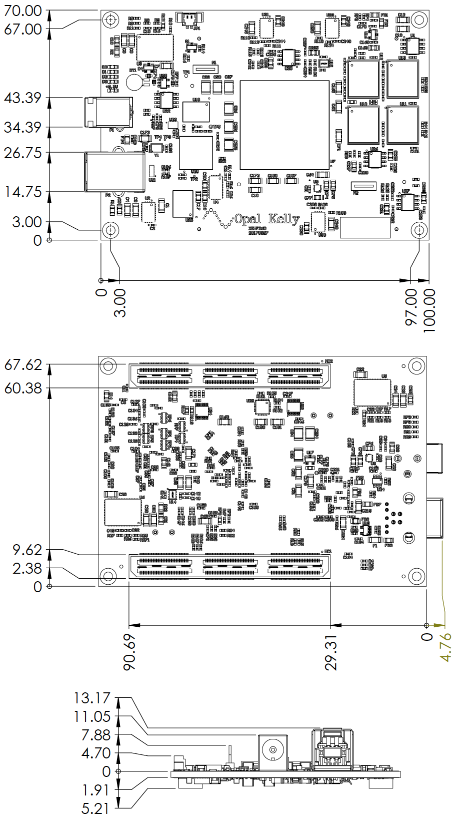
PCB Footprint
The XEM7360 PCB is 100mm x 70mm with four mounting holes (M2 metric screws) spaced as shown in the figures below. These mounting holes are electrically isolated from all signals on the XEM7360. The two connectors (USB and DC power) overhang the PCB by approximately 1.3mm in order to accommodate mounting within an enclosure.
The XEM7360 has two high-density 0.5mm connectors providing access to 193 I/O, 8 multi-gigabit transceivers, and multiple electrically-programmable adjustable voltages.
Mechanical Drawing
The mechanical drawing below may be used for enclosure or mounting hardware design. 3D Models are also available in SolidWorks, STEP, and IGES formats.
All dimensions in mm.
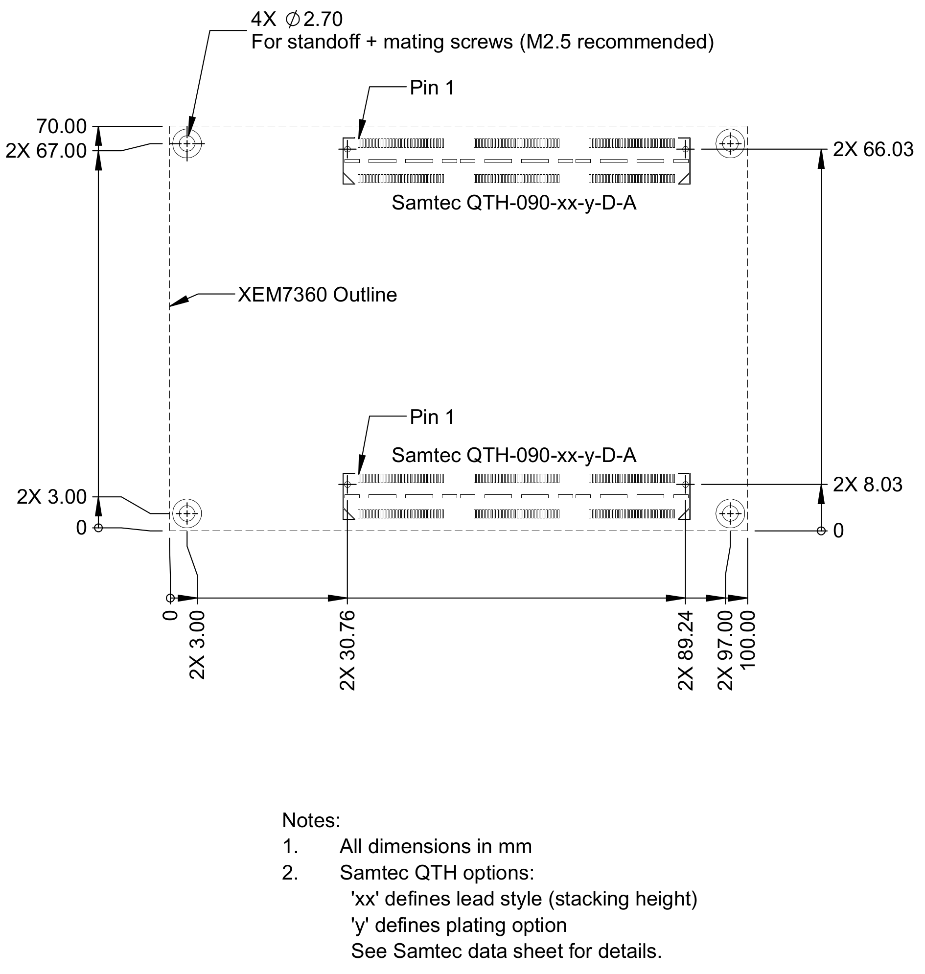
Mating Board Diagram
Use the mating diagram below to orient and design peripheral mating hardware. Note that this is a top-down view and mates to the bottom of the XEM7360. This design is realized in Altium CAD drawings in the corresponding breakout board which are available through Pins Downloads.
For Samtec connector details, drawings, models, and landing patterns, please visit Samtec’s website.
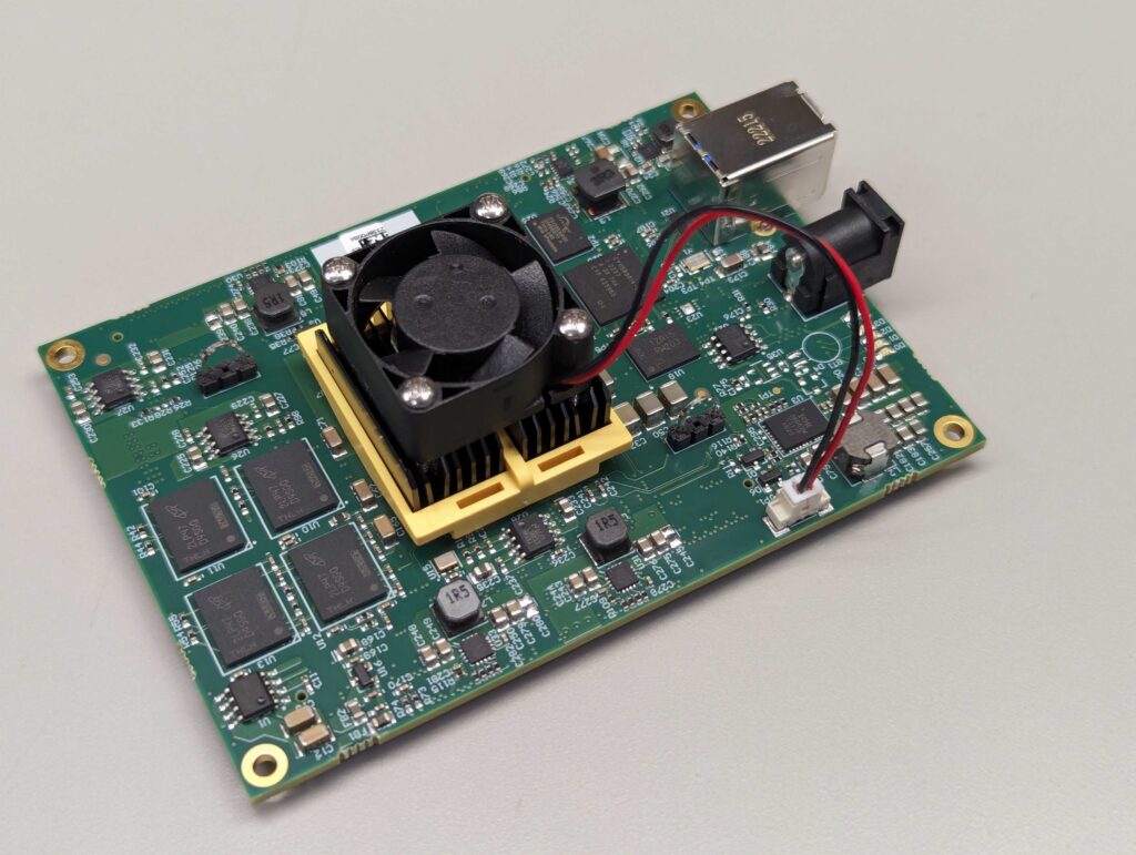
Heatsink
The device has been fitted with two heatsink anchors, proximate to the FPGA for mounting a passive or active heat sink. New revisions of the PCB allow for a BGA clip on fansink to be used. The following heat sinks have been tested with the XEM7360.
| MANUFACTURER | PART NUMBER | DESCRIPTION | Compatibility |
|---|---|---|---|
| Opal Kelly Incorporated | FANSINK-08 | Custom BGA clip on heatsink with fan | Rev EXX and newer |
| Opal Kelly Incorporated | FANSINK-30X30-MC | Custom anchor clip heatsink with fan | Rev EXX and older |
The heat sinks above were custom built based on design specifications provided by Opal Kelly to mate to the XEM7360. They includes a small fan which connects to the fan controller on-board for manual or automatic fan control. They are available for purchase directly from Opal Kelly.
Installation
The thermal transfer material on the bottom of the heatsink is a phase change medium that is sandwiched to the FPGA surface and softens for conductivity under the heat and pressure of attachment.
FANSINK-08
The BGA clip heatsink has a plastic clip that grips onto the BGA package itself. Before installation, remove the protective plastic from the thermal transfer material on the bottom of the heatsink. Place the heatsink on the board in the orientation shown in the image below. Clip the plastic BGA clip over one side of the FPGA. Press the clip horizontally towards the un-clipped side with firm but gentle pressure, at the same time you press down on the un-clipped side, to get the second clip over the other edge of the FPGA and to secure the heatsink in place.
FANSINK-30X30-MC
To install, you should be able to hook one end of the clip on one of the anchors, then, while applying even pressure to the heatsink to make sure the FPGA itself has even pressure, hold that in place while you press the other end of the clip into the anchor.
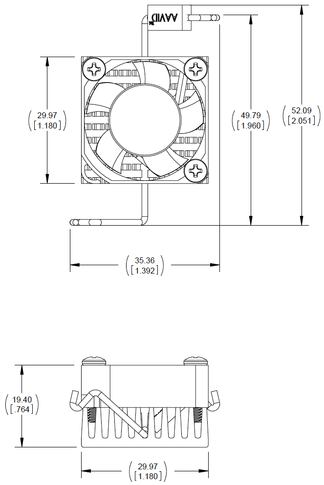
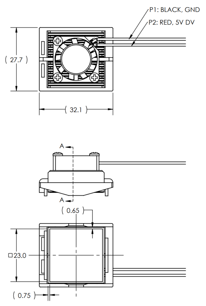
Dimensions
Note that all dimensions are in (mm) with dimensions in inches in brackets.
FANSINK-08
This fansink is Radian part number FJ27/1.3+Y+T725, with a customized power connector.
FANSINK-30X30-MC