DDR3 Memory Walkthrough
Configuring the MIG
Begin by selecting the “Memory Interface Generator (MIG 7 Series)” from the Vivado IP Catalog. On the MIG configuration window that appears:
- Select Next to begin configuration.
- Select the “Create Design” option and click Next again.
- Click Next and select the DDR3 SDRAM controller type then click Next once more.
Options Page 1
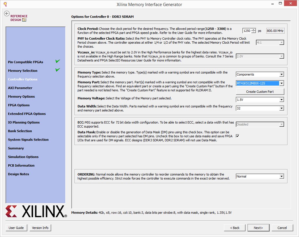
The first Controller Options page requires the following settings:
- Enter a clock period of 1250 ps (corresponding to 800MHz).
- Select the MT41K512M8XX-125 part from the Memory Part dropdown.
- Select a Memory Voltage of 1.5V.
- Enter a Data Width of 32.
- Enable the Data Mask setting.
Options Page 2
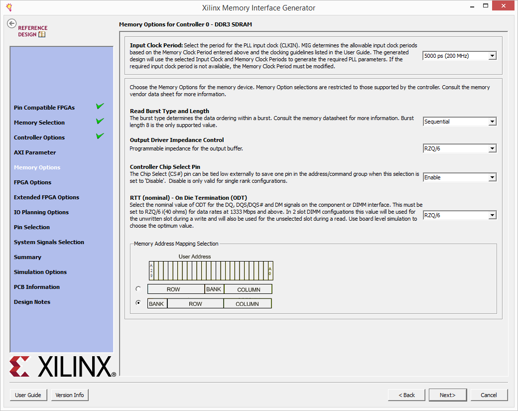
The second Controller Options Page requires the following settings:
- Set the Input Clock Period to 5000 ps (200 MHz).
- Set the Read Burst Type and Length to Sequential.
- Select RZQ/6 for both the Output Driver Impedance Control and the RTT (nominal) – On Die Termination (ODT).
- Enable the Controller Chip Select Pin.
- Select a BANK | ROW | COLUMN address mapping.
Options Page 3
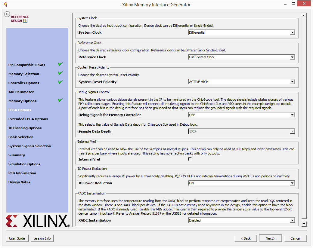
The third Controller Options Page requires the following settings:
- Set the system clock to use a Differential input
- Use the system clock for the reference clock
- Change the system reset polarity to ACTIVE HIGH
- Turn on IO Power Reduction
- Enable the XADC Instantiation
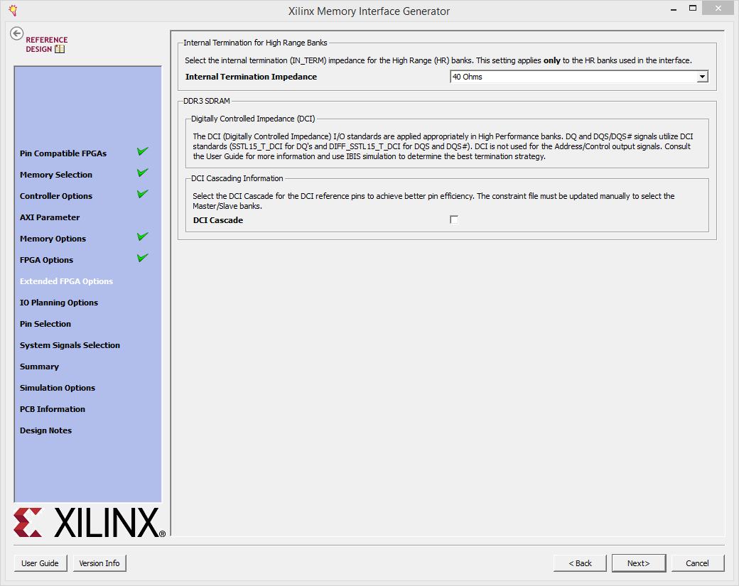
Options Page 4
The fourth Controller Options page requires setting the Internal termination Impedance to 40 ohms.
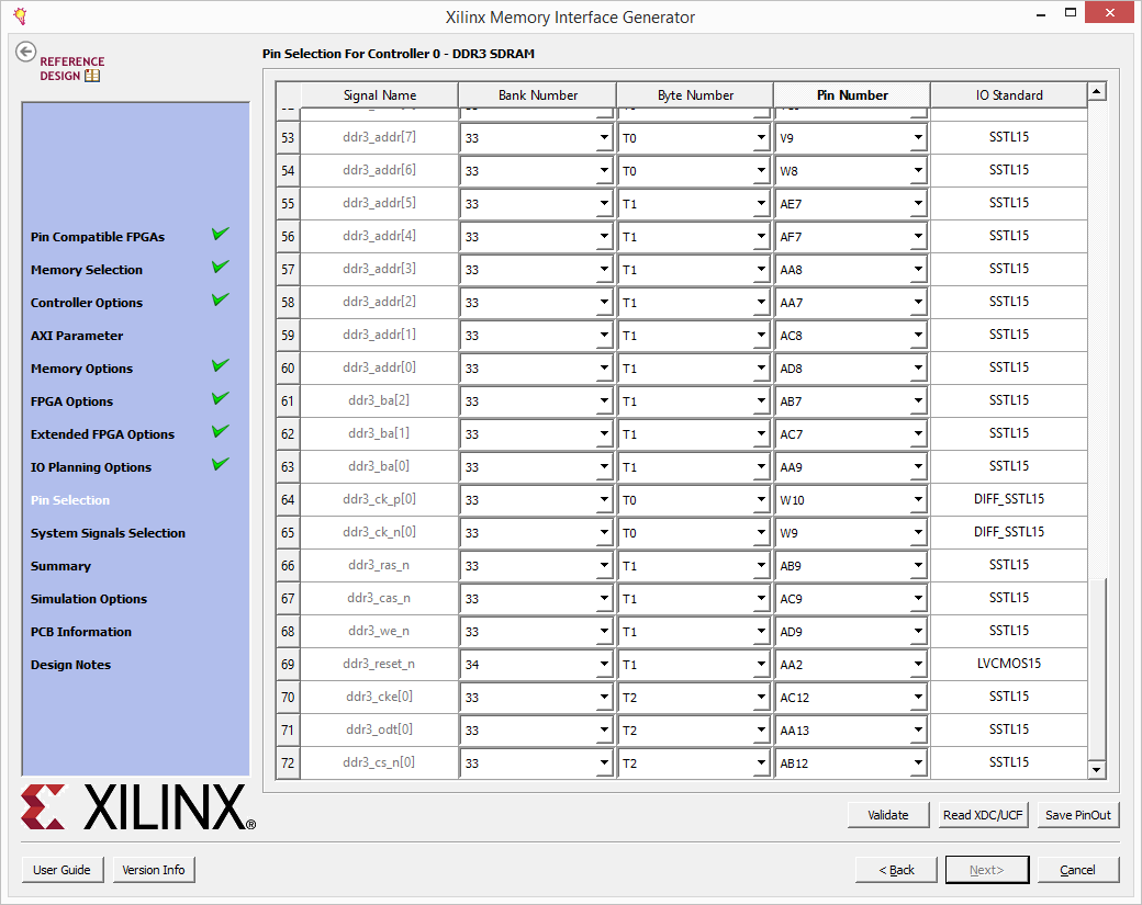
Pin Out Verification
Select the Fixed Pin Out and on the next screen enter the pin number for each pin corresponding to the tables at the top of the DDR3 Memory page. When finished click “Validate” to ensure that the entered pinout is valid.
System Signals Selection
Select the AB11/AC11(CC_P/N) pair for sys_clk_p/n (this is on bank 33). Click Next.
Continue through the configuration utility and click Generate on the final page to generate the Memory Controller IP.