BRK8310 Breakout Board
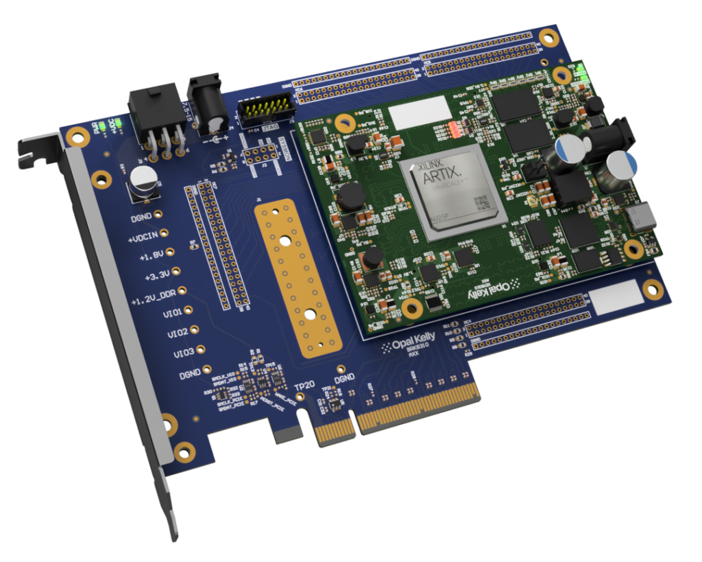
Peripherals and Connectors
The table below summarizes the various connectors on the BRK8310. The XEM8310 Pin List has connection information in the “BRK8310” column. Additionally, please refer to the schematics and layout available on the Downloads section of the Pins website for detailed connection diagrams.
| CONNECTOR TYPE | REFDES | FPGA CONNECTION | I/O Count | |
|---|---|---|---|---|
| PCIE | J6 | GTY224, GTY225 | TxRx 0-3 | |
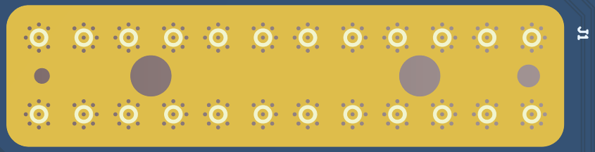
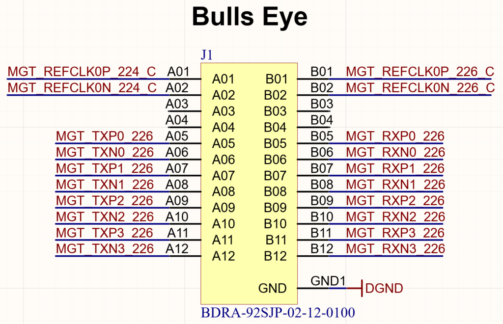
| Samtec Bulls Eye | J1 | GTY226 | TxRx 0-3 | |
| 2mm Header | MC4 | Bank 64 | 38 | |
| 2mm Header | MC5 | Bank 64, 84 | 38 | |
| 2mm Header | MC6 | Bank 86, 87 | 40 | |
| 2mm Header | MC7 | Bank 67, 86 | 33 | |
| JTAG Header | J3 | JTAG Pins |
Power Connectors
Barrel Jack Power Connector
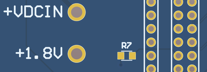
The barrel jack power connector on the BRK8310 is part number PJ-102AH from CUI, Inc. It is a standard “canon-style” 2.1mm / 5.5mm jack. The outer ring is connected to DGND, the center pin is +VDCIN. The PJ-102AH jack is rated for 5 A maximum continuous current.
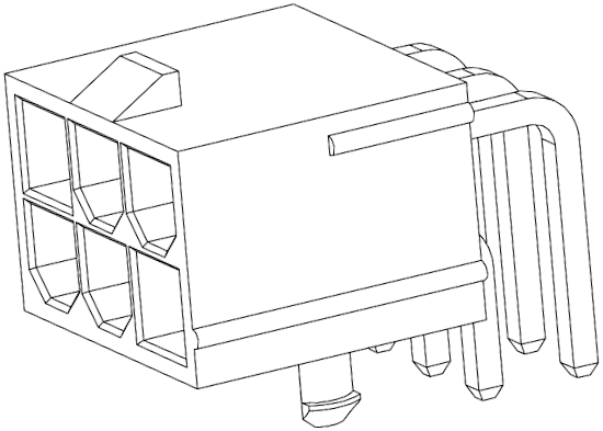
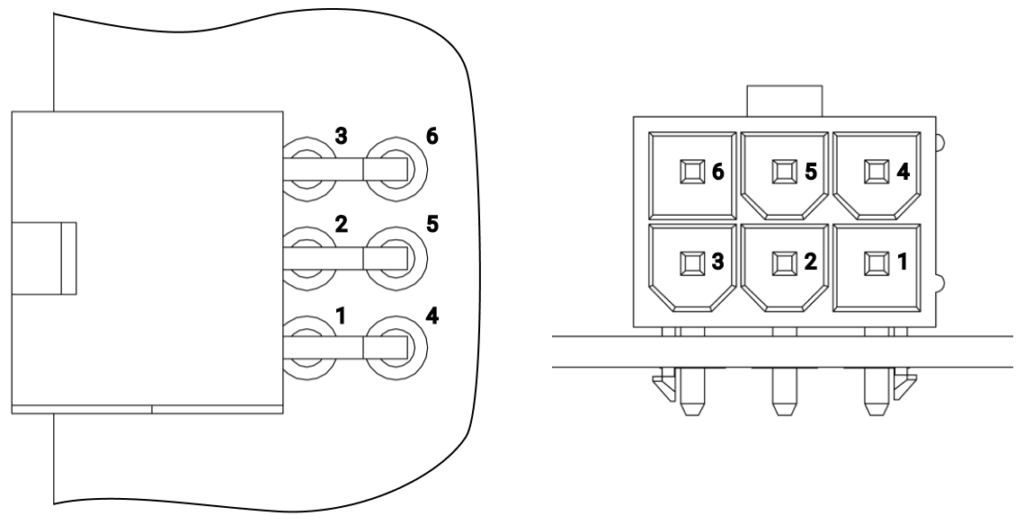
6-Pin Power Connector
The 6-pin connector is a PCIe-style power connector from Molex, part number 0455580003. Pins 1-3 are connected to +VDCIN, and pins 4-6 are connected to DGND. Maximum current is 24 A (8 A per pin).
JTAG
The BRK8310 includes a 2×7 pin 2mm JTAG header that is compatible with many JTAG programmers.
PCIE Connector Fin
The BRK8310 is designed to slot into a standard computer PCIE x8 and larger connector. This allows for a high bandwidth PCIE host connection.
PCIE Lanes
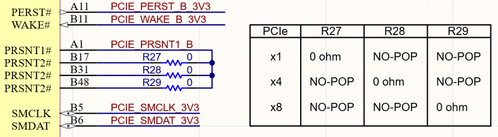
The BRK8310 supports up to a x8 PCIE connection and is configured for x8 lanes by default. This is the maximum PCIE width supported by Artix UltraScale+. For more information see the PG213 section ‘Artix UltraScale+ Devices Available GT Quads’.
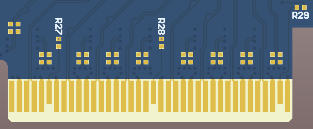
A x1 or x4 lane connection can be configured if required. To change the configured number of lanes, place the PCIE_PRSNT jumper resistor in the appropriate location as defined in the table on the BRK8310 schematic.
Control Signals
Level shifting of PERST, WAKE and SMBus signals to the host is handled on the BRK8310. Control IO signals across the connector are disabled if either side is unpowered.
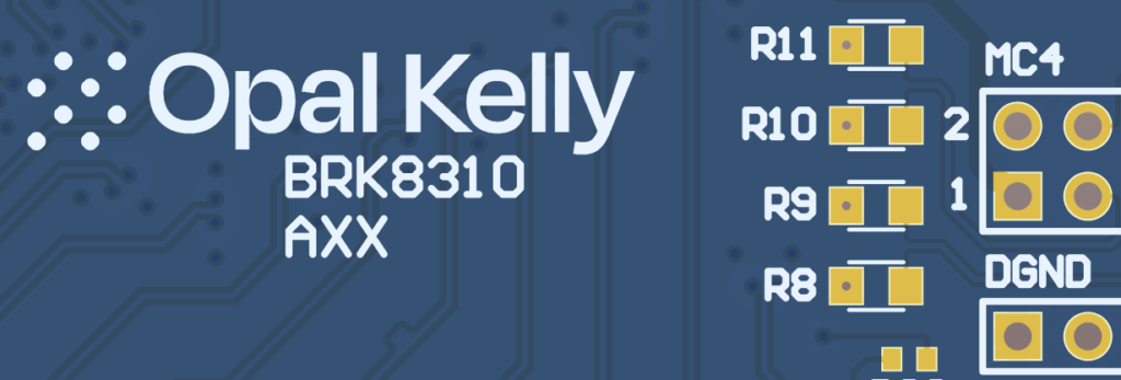
The IO used for these control signals are connected via 0R jumpers that can be removed if the IO is required for another purpose.
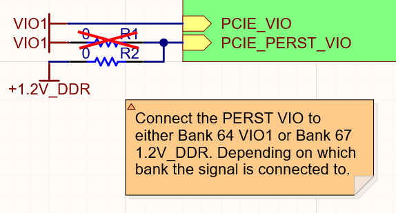
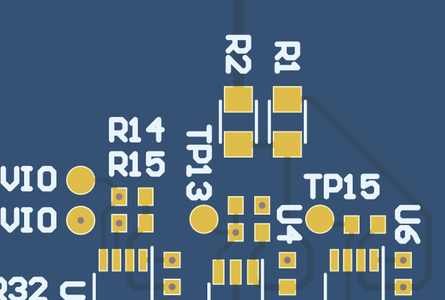
By default the PERST signal is connected to a Bank 67 IO pin. This bank has a fixed IO voltage of 1.2V, and so it is able to operate faster after power on. This is required for a tandem FPGA and host system boot config. Alternatively, PERST can be moved to Bank 64 with the rest of the PCIE control IO by moving resistor jumpers.
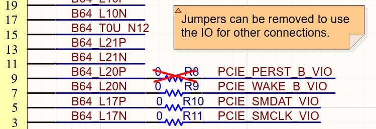

PERST IO level can be set to either VIO1 (Bank 64) or 1.2V via jumper resistors, depending on which IO bank the signal is connected to.
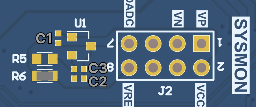
ADC Voltage Reference
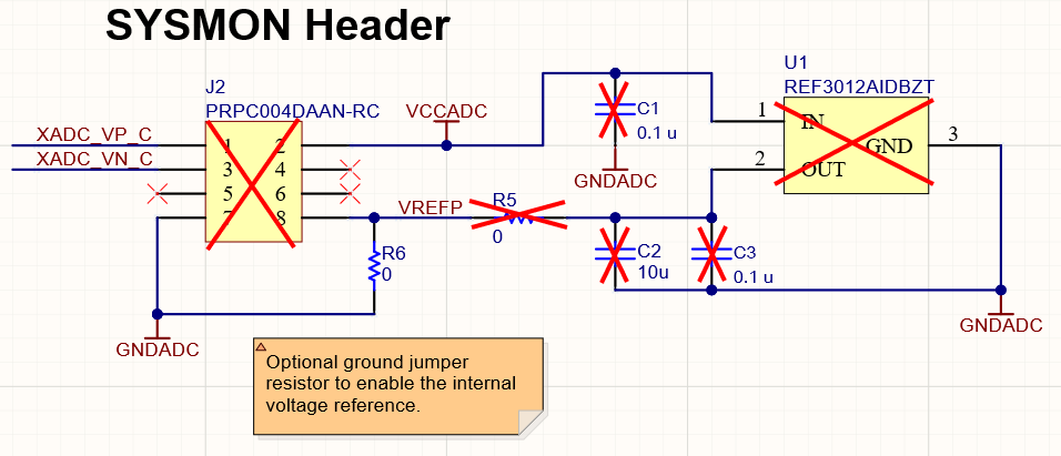
By default BRK8310 includes a 0R jumper that enables the XEM8310 FPGA’s internal ADC voltage reference. However part footprints are included for adding an external high precision reference voltage IC if required.
To use an external 1.25V voltage reference such as REF3012AIDBZT or compatible:
- Remove jumper resistor R6
- Place voltage reference U1
- Place capacitors C1, C2 and C3
- Place jumper resistor R5
Samtec Bulls Eye
The GTY transceiver bank 226 is routed to a Samtec BDRA Bulls Eye high-performance test system footprint. For more information on using this footprint see Samtec’s documentation.
PCIE Bracket
The BRK8310 is designed to slot into a standard x8 or larger PCIE slot. It has mounting holes to attach a standard PCIE bracket for mechanical support. This bracket is available as an optional accessory to the BRK8310.
Impedance and Length Matching
Single-ended fabric I/O are routed to the breakout connectors with 50Ω characteristic impedance. Differential fabric I/O and transceiver signals are routed to the breakout connectors as pairs with 100Ω differential impedance.
Schematic and Design Files
The BRK8310 schematics and design files are available in the Downloads section of the Pins website.
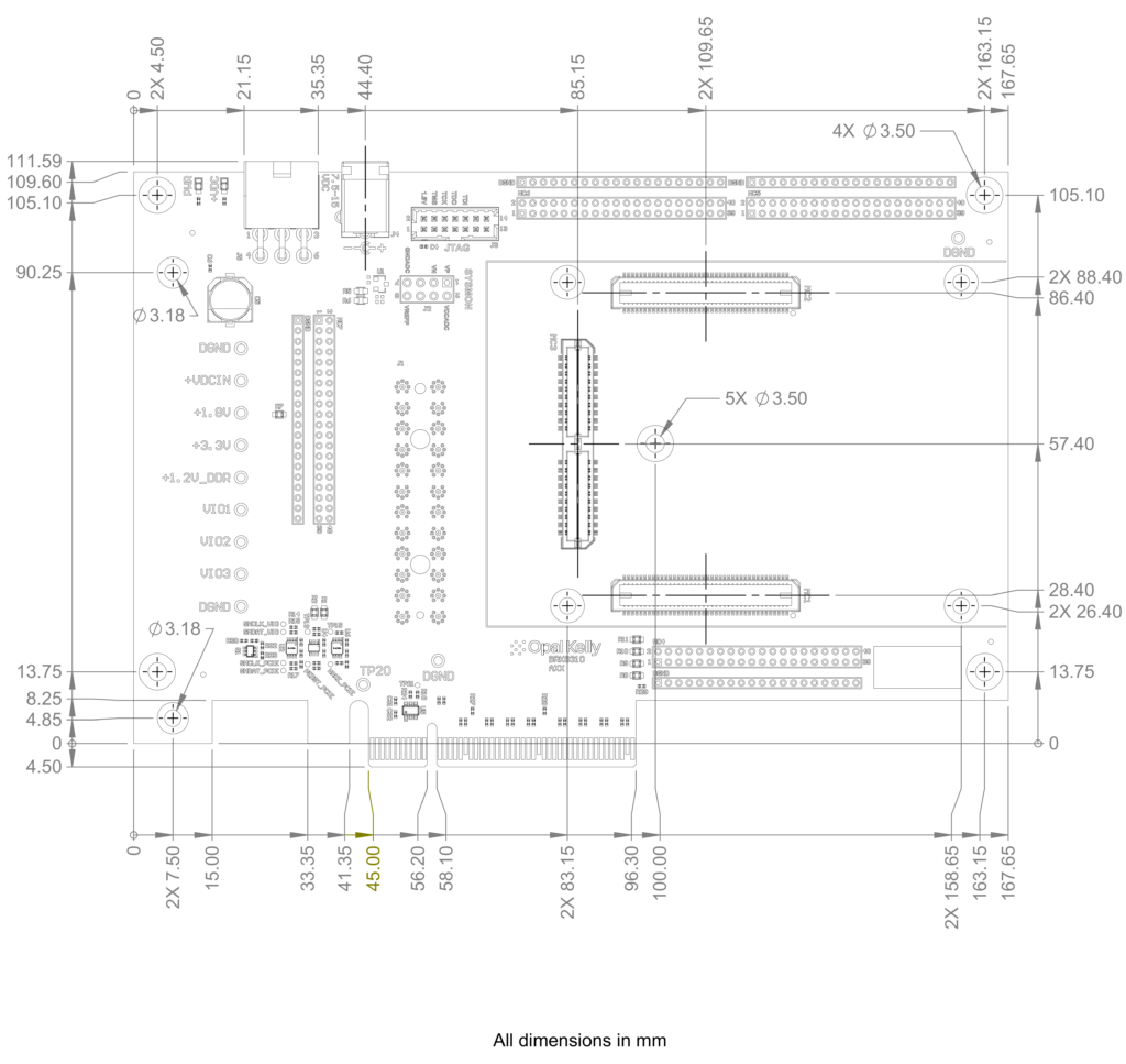
Mechanical Drawing
The mechanical drawing below may be used for enclosure or mounting hardware design. 3D Models are also available in SolidWorks, STEP, and IGES formats.