JTAG
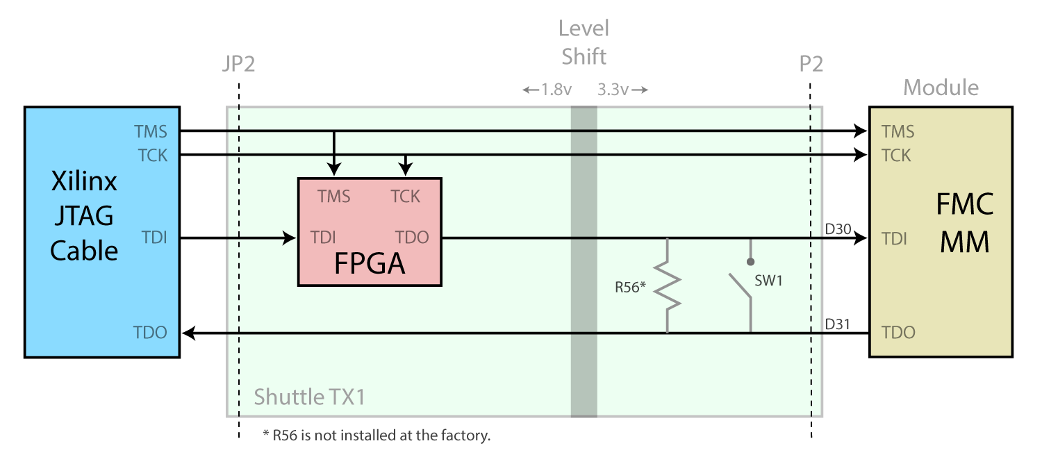
The JTAG connections on the FPGA are wired directly to the 2mm header JP2 on the XEM7350 to facilitate FPGA configuration and ChipScope usage using a Xilinx JTAG cable. The JTAG interface presented at JP2 is a 1.8v interface.
By design, the FMC module is intended to complete the JTAG chain. If a mezzanine module is not present, or does not properly complete the chain, the chain may be bypassed using SW1 or, optionally, installing a 0-Ω resistor at location R56.
To accommodate the FMC requirement that the JTAG chain operate at 3.3v, level shifters are present on-board. Installing a 0-Ω resistor at location R73 keeps the entire chain at 1.8v, but U33 must also be removed to avoid drive contention from the 3.3v side to the 1.8v side.
The JTAG connector on the XEM7350 is Molex 87831-1420 and is not inserted in the factory default configuration.
The JTAG connector pinout is as follows:
| CONNECTOR PIN | JTAG SIGNAL | CONNECTOR PIN | JTAG SIGNAL |
|---|---|---|---|
| 1 | GND | 2 | +1.8V (Vref) |
| 3 | GND | 4 | JTAG_TMS |
| 5 | GND | 6 | JTAG_TCK |
| 7 | GND | 8 | JTAG_TDO |
| 9 | GND | 10 | JTAG_TDI |
| 11 | GND | 12 | NC |
| 13 | GND | 14 | NC |