Expansion Connectors
Opal Kelly Pins is an interactive online reference for the expansion connectors on all Opal Kelly FPGA integration modules. It provides additional information on pin capabilities, pin characteristics, and PCB routing.
Pins can also generate constraint files (UCF) and help you map your HDL net names to FPGA pin locations automatically.
The Pins reference for the XEM6310 may be found at the link to the right.
Expansion Connectors
Two high-density, 80-pin expansion connectors are available on the bottom-side of the XEM6310 PCB. These expansion connectors provide user access to several power rails on the XEM6310, the JTAG interface on the FPGA, and 124 non-shared I/O pins on the FPGA, including several GCLK inputs.
The connectors on the XEM6310 are Samtec part number: BSE-040-01-F-D-A. The table below lists the appropriate Samtec mating connectors along with the total mated height.
| SAMTEC PART NUMBER | MATED HEIGHT |
|---|---|
| BTE-040-01-F-D-A | 5.00mm (0.197”) |
| BTE-040-02-F-D-A | 8.00mm (0.315”) |
| BTE-040-03-F-D-A | 11.00mm (0.433”) |
| BTE-040-04-F-D-A | 16.10mm (0.634”) |
| BTE-040-05-F-D-A | 19.10mm (0.752”) |
JP1
JP1 is an 80-pin high-density connector providing access to FPGA Banks 0, 1, and 2. Several pins (42, 44, 59, 61, 64, 66, 77, and 79) of this connector are wired to global clock inputs on the FPGA and can therefore be used as inputs to the global clock network.
Pin mappings for JP1 are listed on the pins page linked above. For each pin, the corresponding board connection is listed. For pins connected to the FPGA, the corresponding FPGA pin number is also shown. Finally, for pins routed to differential pair I/Os on the FPGA, the FPGA signal names and routed track lengths have been provided to help you equalize lengths on differential pairs.
Note that JP1 pins 8, 10, 12 are attached to FPGA Bank 2 which is powered as a 1.8 V bank. This may not be changed.
JP2
JP2 is an 80-pin high-density connector providing access to FPGA Bank 1 (except for pin JP2-11 which is on Bank 2). Several pins (38, 40, 54, 58, 59, 61, 77, and 79) of this connector are wired to global clock inputs on the FPGA and can therefore be used as inputs to the global clock network.
Pin JP2-10 is connected to the Vref pins of Bank 1.
Pin mappings for JP2 are listed on the pins page linked above. For each pin, the corresponding board connection is listed. For pins connected to the FPGA, the corresponding FPGA pin number is also shown. Finally, for pins routed to differential pair I/Os on the FPGA, the FPGA signal names and routed track lengths have been provided to help you equalize lengths on differential pairs.
Note that JP2 pin 11 is attached to FPGA Bank 2 which is powered as a 1.8 V bank. This may not be changed.
Setting I/O Voltages
The Spartan-6 FPGA allows users to set I/O bank voltages in order to support several different I/O signal standards. This functionality is supported by the XEM6310 by allowing the user to connect independent supplies to the FPGA VCCO pins on two of the FPGA banks.
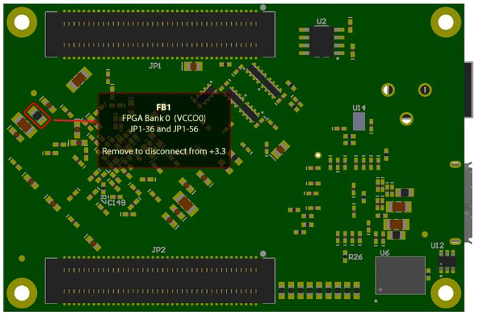
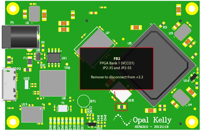
By default, ferrite beads have been installed that attach each VCCO bank to the +3.3VDD supply. If you intend to supply power to a particular I/O bank, you MUST remove the appropriate ferrite beads. Power can then be supplied through the expansion connectors.
The table below lists details for user-supplied I/O bank voltages
| I/O BANK | EXPANSION PINS | FERRITE BEAD |
|---|---|---|
| 0 | JP1-36, 56 | FB1 |
| 1 | JP2-35, 55 | FB2 |
Ferrite Bead Locations
Considerations for Differential Signals
The XEM6310 PCB layout and routing has been designed with several applications in mind, including applications requiring the use of differential (LVDS) pairs. Please refer to the Xilinx Spartan-6 datasheet for details on using differential I/O standards with the Spartan-6 FPGA.
FPGA I/O Bank Voltages
In order to use differential I/O standards with the Spartan-6, you must set the VCCO voltages for the appropriate banks to 3.3 V (LVDS_33) or 2.5 V (LVDS_25) according to the Xilinx Spartan-6 datasheet. Please see the section above entitled “Setting I/O Voltages” for details.
Characteristic Impedance
The characteristic impedance of all routes from the FPGA to the expansion connector is approximately 50-Ω.
Differential Pair Lengths
In many cases, it is desirable that the route lengths of a differential pair be matched within some specification. Care has been taken to route differential pairs on the FPGA to adjacent pins on the expansion connectors whenever possible. We have also included the lengths of the board routes for these connections to help you equalize lengths in your final application. Due to space constraints, some pairs are better matched than others.
Reference Voltage Pins (Vref)
The Xilinx Spartan-6 supports externally-applied input voltage thresholds for some input signal standards. The XEM6310 supports these Vref applications for banks 0 and 1:
For Bank 0, the four Vref pins are routed to expansion connector JP1 on pins 48, 51, 62, and 65. Note that all four must be connected to the same voltage for proper application of input thresholds. Please see the Xilinx Spartan-6 documentation for more details.
For Bank 1, the four Vref pins are connected to a single pin on expansion connector JP2, pin 10.