Expansion Connectors
Opal Kelly Pins is an interactive online reference for the expansion connectors on all Opal Kelly FPGA integration modules. It provides additional information on pin capabilities, pin characteristics, and PCB routing.
Pins can also generate constraint files (XDC) and help you map your HDL net names to FPGA pin locations automatically.
The Pins reference for the XEM7310 may be found at the link to the right.
Connector Details
Two high-density, 80-pin expansion connectors are available on the bottom-side of the XEM7310 PCB. These expansion connectors provide user access to several power rails on the XEM7310, the JTAG interface on the FPGA, and 126 I/O pins on the FPGA, including several MRCC clock inputs.
The connectors on the XEM7310 are Samtec part number: BSE-040-01-F-D-A. The table below lists the appropriate Samtec mating connectors along with the total mated height.
| SAMTEC PART NUMBER | MATED HEIGHT |
|---|---|
| BTE-040-01-F-D-A | 5.00mm (0.197”) |
| BTE-040-02-F-D-A | 8.00mm (0.315”) |
| BTE-040-03-F-D-A | 11.00mm (0.433”) |
| BTE-040-04-F-D-A | 16.10mm (0.634”) |
| BTE-040-05-F-D-A | 19.10mm (0.752”) |
MC1
MC1 is an 80-pin high-density connector providing access to FPGA Banks 34 and 13. Several pins of this connector are wired to clock inputs on the FPGA, see the table below and the AMD Artix-7 documentation for more details.
Pin mappings for MC1 are listed on the pins page linked above. For each pin, the corresponding board connection is listed. For pins connected to the FPGA, the corresponding FPGA pin number is also shown. Finally, for pins routed to differential pair I/Os on the FPGA, the FPGA signal names and routed track lengths have been provided to help you equalize lengths on differential pairs.
Note that MC1 pins 64 and 66-76 are attached to FPGA Bank 13 which is powered as a 3.3 V bank. This may not be changed.
MC2
MC2 is an 80-pin high-density connector providing access to FPGA Bank 35 and 13. Several pins of this connector are wired to clock inputs on the FPGA, see the table below and the AMD Artix-7 documentation for more details.
Pin mappings for MC2 are listed on the pins page linked above. For each pin, the corresponding board connection is listed. For pins connected to the FPGA, the corresponding FPGA pin number is also shown. Finally, for pins routed to differential pair I/Os on the FPGA, the FPGA signal names and routed track lengths have been provided to help you equalize lengths on differential pairs.
Note that MC2 pins 64 and 66-76 are attached to FPGA Bank 13 which is powered as a 3.3 V bank. This may not be changed.
FPGA Bank Connections
| FPGA BANK | Bank Type | Bank VOLTAGE | MCX | VIO | I/O AVAILABLE |
|---|---|---|---|---|---|
| 13 | HR | 3.3 V (Fixed) | MC1 and MC2 | N/A | 26 |
| 34 | HR | 3.3V (1.14 – 3.465V if external) | MC1 | VCCO_MC1 | 48 |
| 35 | HR | 3.3V (1.14 – 3.465V if external) | MC2 | VCCO_MC2 | 50 |
Clock Pins
Clock Input Pins
Available clock pins are illustrated in the table below. All pins listed are multi-region clock pins.
| FPGA BANK | FPGA PINS | MCX PINS |
|---|---|---|
| Bank 34 MRCC | V4 W4 | MC1:77 MC1:79 |
| Bank 34 MRCC | R4 T4 | MC1:32 MC1:34 |
| Bank 35 MRCC | H4 G4 | MC2:77 MC2:79 |
| Bank 35 MRCC | K4 J4 | MC2:63 MC2:65 |
| Bank 13 MRCC | V13 V14 | MC2:71 MC2:73 |
SYS_CLK Output Pins
The SYS_CLK_MC1 and SYS_CLK_MC2 expansion connector nets are so named for compatibility with legacy products. They can be used as clock outputs to support connections to legacy carrier boards. On the XEM7310 they are directly connected to the FPGA I/O pins listed on the Pins Reference sheet and can be used as general I/O. There is no extra hardware attached to them.
FPGA Bank Voltage Configuration
The table below describes the power supply configuration of the FPGA banks on the XEM7310. Note that the bank voltages for banks 13, 14, 15, and 16 may not be changed. VCCO_MC1 and VCCO_MC2 are connected to 3.3v by factory default.
| BANK | POWER SUPPLY |
|---|---|
| 13 | 3.3v |
| 14 | 1.8v |
| 15 | 1.5v |
| 16 | 1.5v |
| 34 | VCCO_MC1 (3.3v Default) |
| 35 | VCCO_MC2 (3.3v Default) |
Setting the Expansion Connector I/O Voltages
The Artix-7 FPGA allows users to set I/O bank voltages in order to support several different I/O signal standards. This functionality is supported by the XEM7310 by allowing the user to connect independent supplies to the FPGA VCCO pins on two of the FPGA banks.
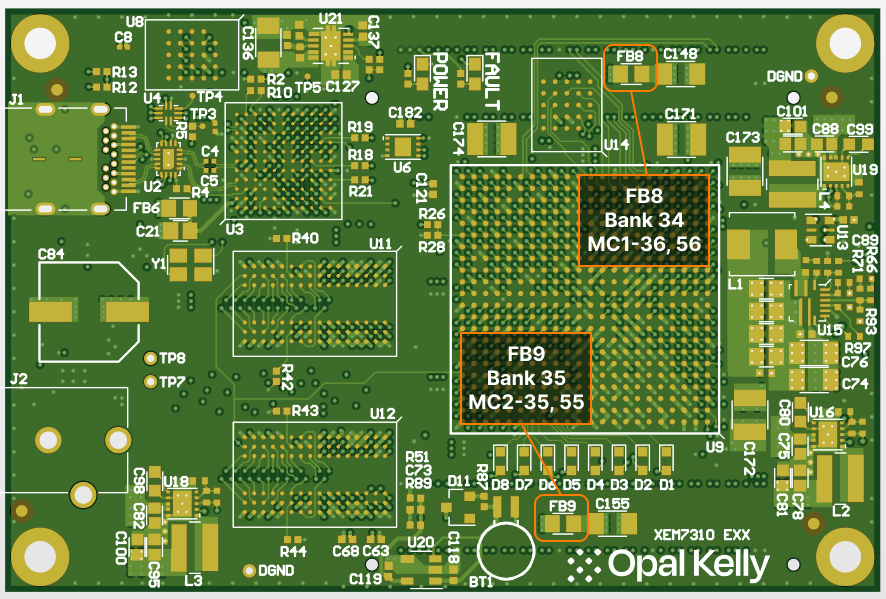
By default, ferrite beads (P/N Steward HZ0402B102R-10) have been installed that attach each VCCO bank to the +3.3VDD supply. If you intend to supply power to a particular I/O bank, you MUST remove the appropriate ferrite beads. Power can then be supplied through the expansion connectors.
The table below lists details for user-supplied I/O bank voltages
| I/O BANK | VCCO EXPANSION PINS | FERRITE BEAD | Voltage Range |
|---|---|---|---|
| 34 | VCCO_MC1 on pins MC1-36 and MC1-56 | FB8 | 1.14 – 3.465V |
| 35 | VCCO_MC2 on pins MC2-35 and MC2-55 | FB9 | 1.14 – 3.465V |
For pin connection details see the Pins page.
For information on FPGA power supply startup sequencing when using external I/O voltages, see Powering the XEM7310.
Ferrite Bead Locations
FPGA Power-On Sequencing with External VCCO
The Artix-7 family of devices has the following recommended power supply startup sequence:
- VCCINT/VCCBRAM
- VCCAUX
- VCCO
This sequence achieves minimum current draw and ensures I/O are tristated at power-on. For more information see the “Power-On/Off Power Supply Sequencing” section in the Artix-7 FPGA Data Sheet (DS181).
To meet this sequencing recommendation when applying external VCCO power supplies, the external system should monitor the XEM7310 +1.8VDD supply on mezzanine connector MC1, pin 7. This on-board voltage rail powers the FPGA VCCAUX pins directly. After the +1.8VDD rail is within regulation (within ±10%, for example), the external system may apply VCCO to the module.
XADC
The AMD Artix-7 XADC dedicated differential analog input channel VP and VN pins are each routed through a 1kΩ resistor to the MC1 connector. There is a 680 pF capacitor installed across the two FPGA pins for decoupling. The VCCADC input is connected through a ferrite bead and with decoupling capacitors to 1.8V.
| FPGA FUNCTION | FPGA PIN | MC1 PIN | RESISTOR REFDES |
|---|---|---|---|
| ADC_VN_0 | M9 | 10 | R33 |
| ADC_VP_0 | L10 | 12 | R32 |
Considerations for Differential Signals
The XEM7310 PCB layout and routing has been designed with several applications in mind, including applications requiring the use of differential (LVDS) pairs. Please refer to the AMD Artix-7 datasheet for details on using differential I/O standards with the Artix-7 FPGA.
FPGA I/O Bank Voltages
In order to use differential I/O standards with internal termination on the Artix-7, you must set the VCCO voltages for the appropriate banks to 2.5V according to the AMD Artix-7 datasheet.
Because the bank 13 VCCO is fixed at 3.3V, it’s use of LVDS is limited. For more information on using LVDS with bank 13 see the LVDS and LVDS_25 (Low Voltage Differential Signaling) section of 7 Series FPGAs SelectIO Resources User Guide (UG471).
Characteristic Impedance
The characteristic impedance of all routes from the FPGA to the expansion connector is approximately 50Ω.
Differential Pair Lengths
In many cases, it is desirable that the route lengths of a differential pair be matched within some specification. Care has been taken to route differential pairs on the FPGA to adjacent pins on the expansion connectors whenever possible. We have also included the lengths of the board routes for these connections to help you equalize lengths in your final application. Due to space constraints, some pairs are better matched than others.
Reference Voltage Pins (Vref)
The AMD Artix-7 supports both internal and externally-applied input voltage thresholds for some input signal standards. The XEM7310 supports these Vref applications for banks 13, 34, and 35. Please see the AMD Artix 7 documentation for more details.
For Bank 34, the two Vref pins are routed to expansion connector MC1 on pins 22 and 52. Note that both pins must be connected to the same voltage for proper application of input thresholds. Please see the AMD Artix-7 documentation for more details.
For Bank 35, the two Vref pins are routed to expansion connector MC2 on pins 21 and 57. Note that both pins must be connected to the same voltage for proper application of input thresholds. Please see the AMD Artix-7 documentation for more details.
For Bank 13, the single Vref pin is routed to expansion connector MC2 on pin 74. Please see the AMD Artix-7 documentation for more details.
VCCBATT Pin
MC2 has an optional connection to the FPGAs VCCBATT pin E12. By default this MC2 pin is not connected, and the FPGA VCCBATT pin E12 is connected to GND via the 0 Ohm resistor R89. For external access to VCCBATT remove R89 and place a 0 Ohm resistor on R51.
For more information on VCCBATT see Encryption Key Storage.
I/O State at Power On
AMD Artix-7 FPGAs support a weak pull-up state on all I/O pins from power on until first configuration. This behavior is controlled by the PUDC_B pin. By default the XEM7310 holds the PUDC_B pin high with a 1kΩ resistor at R26, disabling the weak pull-up on all I/O pins at power on. This behavior can be changed by inserting a 0Ω resistor at R28 and removing the 1kΩ resistor at R26, forcing the PUDC_B pin to ground.