Powering the XEM7310
The XEM7310 requires a clean, filtered, DC supply within the range of 4.5 V to 5.5 V. This supply must be delivered through the DC power connector or the expansion connector MC1.
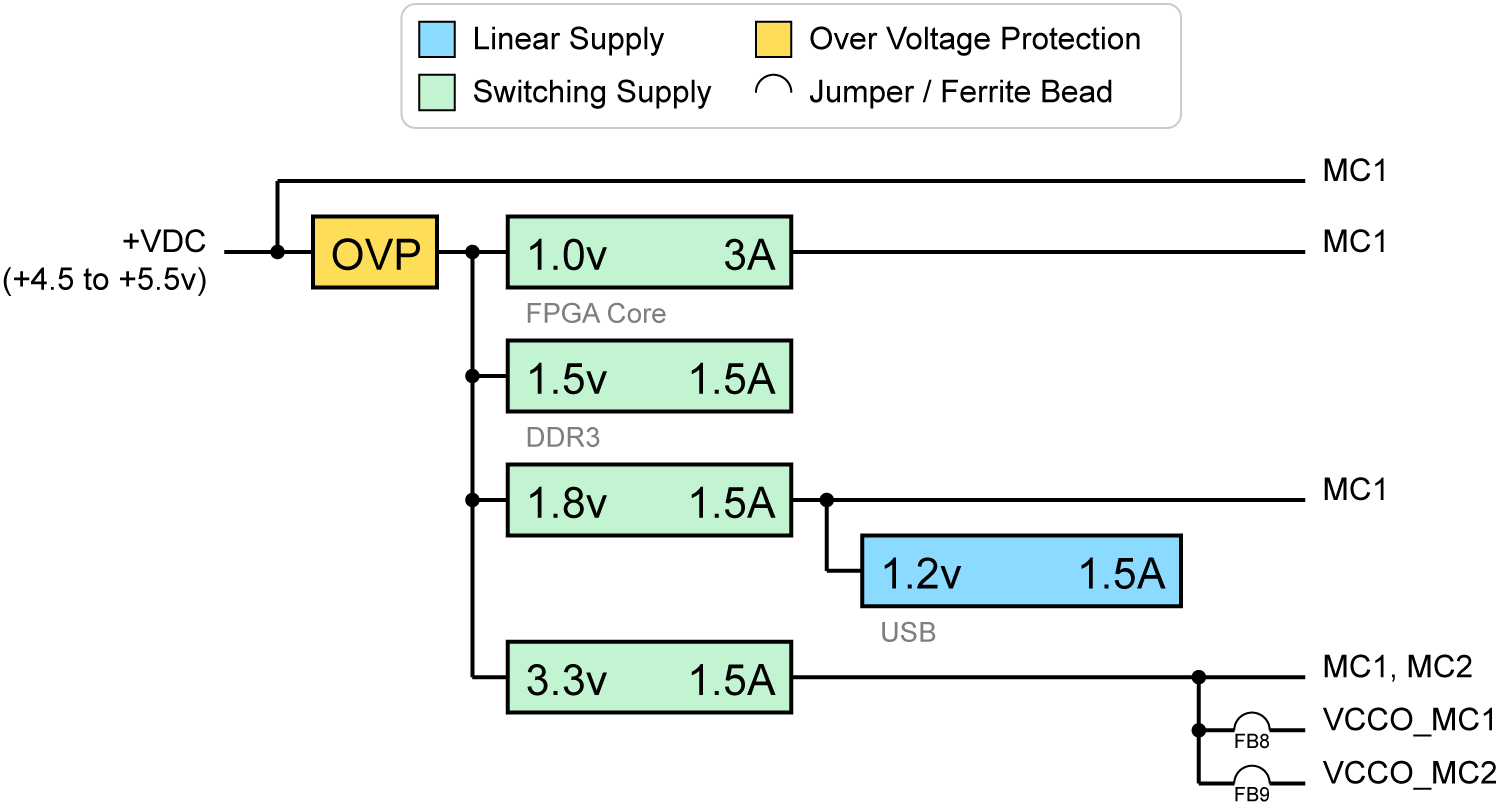
The XEM7310 power distribution system includes several supplies designed to provide suitable, efficient power for several systems and modules. A schematic diagram of the system follows, with input (+VDC) shown to the left and accessible supply rails shown to the right.
Power Supply
The XEM7310 is designed to be operated from a single 5-volt power source supplied through either the DC power jack or the Expansion Connectors on the device. This provides power for the several high-efficiency switching regulators on-board to provide multiple DC voltages for various components on the device as well as three adjustable supplies for the peripheral.
DC Power Connector
The DC power connector on the XEM7310 is part number PJ-102AH from CUI, Inc. It is a standard “canon-style” 2.1mm / 5.5mm jack. This connector is rated for 5A. The outer ring is connected to DGND. The center pin is connected to +VDC.
Expansion Connector
Input power be supplied to the board through the expansion connector. In total the expansion connector can carry 6A for VDCIN. See the VDCIN pin connections in the Pins sheet.
Powering via USB
The XEM7310 has been designed to accept power (+5VDC only) via the USB connector with a small modification. To power from USB, you will need to install a 0 Ω resistor (0603 dimension) at location R62, located on the reverse side of the PCB under the power connector. This will connect the +5VUSB from the USB connector to the +5VDC on the XEM7310.
With this resistor in place, you should not apply +5VDC to an external power connector.
Power Sequencing
The XEM7310MT handles on board power sequencing following guidelines from Xilinx. It is recommended that external I/O signals only be applied after VCCO is powered.
When external VCCO is supplied, those rails should be sequenced after +1.8VDD is fully powered. See the Expansion Connectors page for more information on supplying external VCCO.
+1.0VDD (VCCINT/VCCBRAM) → +1.8VDD (VCCAUX) → +3.3VDD (VCCO_MC1/VCCO_MC2)
+1.0VDD (VCCINT/VCCBRAM) → DDR VDD/DDR VREF
Over Voltage Protection
An electronic fuse on the +VDC input protects the module from over-voltage, under-voltage, and thermal overload conditions. During any one of these conditions, the fuse enters a fault state. In the fault state, the FAULT LED illuminates red and all down-stream power supplies on the module are disabled.
The table below indicates the overvoltage and undervoltage thresholds. The fault state clears automatically when the +VDC input voltage is within the specified range.
| CONDITION | RISING THRESHOLD | FALLING THRESHOLD |
|---|---|---|
| Overvoltage | 5.56 V | 5.12 V |
| Undervoltage | 3.97 V | 3.69 V |
Current Overload
The fuse has an overcurrent limit of approximately 5 A. A current overload condition does not cause the fuse to enter the fault state. Instead, the fuse enters a current limit mode, dissipating power internally to keep the output current at or below the 5 A limit. If the current overload condition continues and the thermal shutdown threshold is reached, the fuse enters the fault state. An automatic retry cycle will clear the fault state when the thermal overload condition no longer exists.
Reverse Voltage
The fuse protects against a reverse voltage/current condition, but the FAULT LED does not illuminate during this condition.
Power Budget
The table below can help you determine your power budget for each supply rail on the XEM7310. All values are highly dependent on the application, speed, usage, and so on. Entries we have made are based on typical values presented in component datasheets or approximations based on Xilinx power estimator results. Shaded boxes represent unconnected rails to a particular component. Empty boxes represent data that the user must provide based on power estimates.
The user may also need to adjust parameters we have already estimated (such as FPGA Vcco values) where appropriate. All values are shown in milliwatts (mW).
| COMPONENT(S) | 1.0V | 1.5V | 1.8V | 3.3V |
|---|---|---|---|---|
| 200 MHz, Misc | 250 | |||
| USB | 500 | |||
| DDR3 | 730 | |||
| FPGA Vccint, Vccbram | ||||
| FPGA Vccaux | ||||
| FPGA Vcco15,16 (DDR3), est. | 280 | |||
| FPGA Vcco14 (USB), est. | 60 | |||
| FPGA Vcco (User I/O) | ||||
| Total (mW) | ||||
| Available (mW) | 3,000 | 2,250 | 2,700 | 4,950 |
Example XEM7310-A200 FPGA Power Consumption
Xilinx Power Estimator version 2015.3 was used to compute the following power estimates for the Vccint supply. These are simply estimates; your design requirements may vary considerably. The numbers below indicate approximately 80% utilization.
| COMPONENT | PARAMETERS | VCCINT | VCCAUX |
|---|---|---|---|
| Clock | 150 MHz GCLK, 220,000 fanout | 570 mW | |
| Logic (DFF) | 150 MHz, 220,000 DFFs | 550 mW | |
| Logic (LUT) | 150 MHz, 100,000 | 550 mW | |
| BRAM | 36-bit, 300 @ 150 MHz | 450 mW | |
| DSP | 150 MHz, 630 slices | 300 mW | |
| Misc. | DCM, PLL, etc. | 10 mW | 500 mW |
| Total | 2,430 mW | 500 mW | |
| Available | 3,000 mW | 2,700 mW |