XEM7001
Specifications
| Host Interface | USB 2.0 Type B FrontPanel Support |
| FPGA | XC7A15T-1FTG |
| Memory | none |
| NV Memory | 4 MiB System Flash (FPGA attached) |
| Oscillator | Programmable, 0.08-200 MHz |
| FPGA I/O Voltage | +3.3V (Fixed) |
| MINIMUM | TYPICAL | MAXIMUM | UNITS | |
|---|---|---|---|---|
| DC Input (USB VBUS) | +4.5 | +5.0 | +5.5 | VDC |
| DC Input Ripple (USB VBUS) | – | – | 50 | mVp-p |
| Operating Temperature | 0 | – | +70 | ºC |
| Storage Temperature | -50 | 0 | +100 | ºC |
| Weight | 24 | grams | ||
| Oscillator Frequency | 0.08 | – | 200 | MHz |
| Oscillator Period Jitter | 250 | ps pk-pk |
PCB Footprint
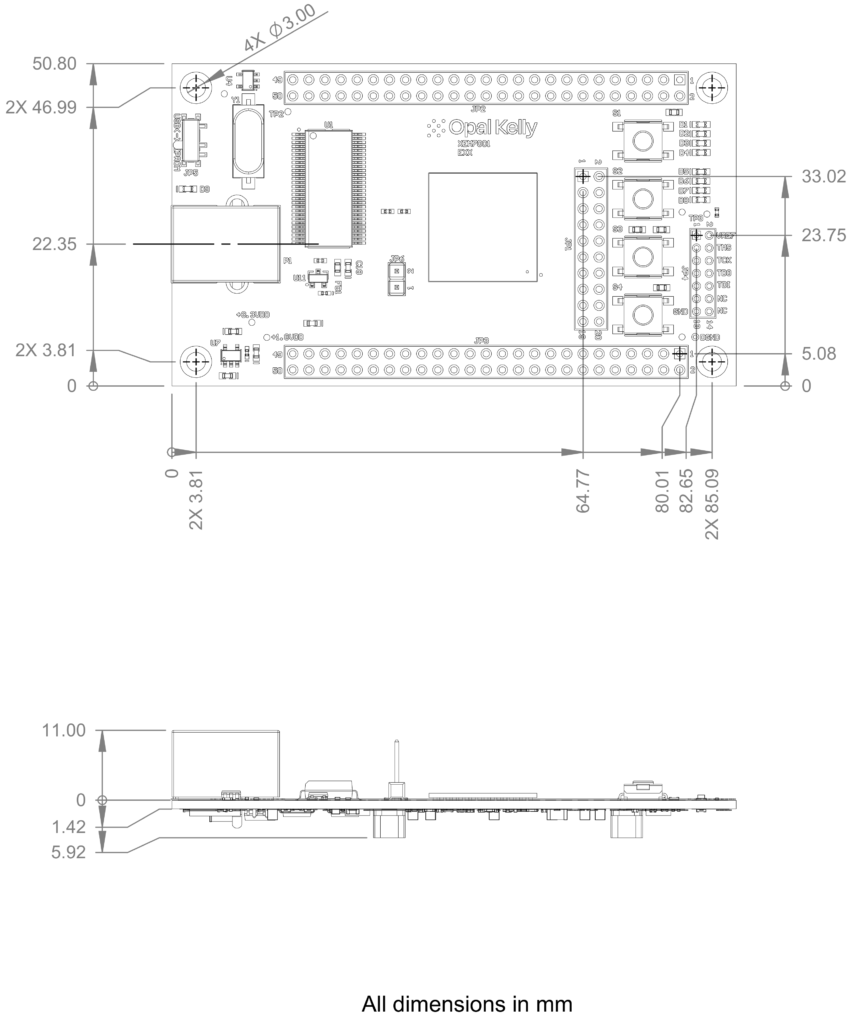
The XEM7001 PCB is 3.5” x 2.0” (88.9mm x 50.8mm) with four mounting holes spaced as shown in the figures below. These mounting holes are electrically isolated (disconnected).
The three FPGA-access ports JP1, JP2, and JP3 are located on a 0.1” grid so that the entire board may be attached to a standard prototyping board. The JTAG header JP4 is also on this grid.
Mechanical Drawing