Specifications
| Host Interface | USB 3.0 Type C, SuperSpeed FrontPanel Support |
| FPGA | XC7A75T-1FGG484C XC7A200T-1FBG484C |
| Memory | 1 GiByte DDR3, 32-bit wide data interface |
| NV Memory | 16 MiB System Flash 16 MiB FPGA Flash |
| Oscillator | 200 MHz |
| FPGA I/O Voltage | See Powering the XEM7310MT |
| MINIMUM | TYPICAL | MAXIMUM | UNITS | |
|---|---|---|---|---|
| DC Input | +4.5 | +5.0 | +5.5 | VDC |
| DC Input Ripple | – | – | 50 | mVp-p |
| Operating Temperature | 0 | – | +70 | ºC |
| Storage Temperature | -50 | 0 | +100 | ºC |
| Weight | 28 | grams | ||
| Oscillator Frequency | 200 | MHz | ||
| Oscillator Freq. Stability | ±50 | ppm | ||
| Oscillator Period Jitter | 2.5 | ps RMS |
| A75 | A200 | |
|---|---|---|
| System Logic Cells | 75,520 | 215,360 |
| CLB Flip-Flops | 94,400 | 269,200 |
| CLB LUTs | 47,200 | 134,600 |
| Max. Distributed RAM (Kb) | 892 | 2,888 |
| Block RAM | 210 blocks (3,780 Kb) | 730 blocks (13,140 Kb) |
| DSP Slices | 180 | 740 |
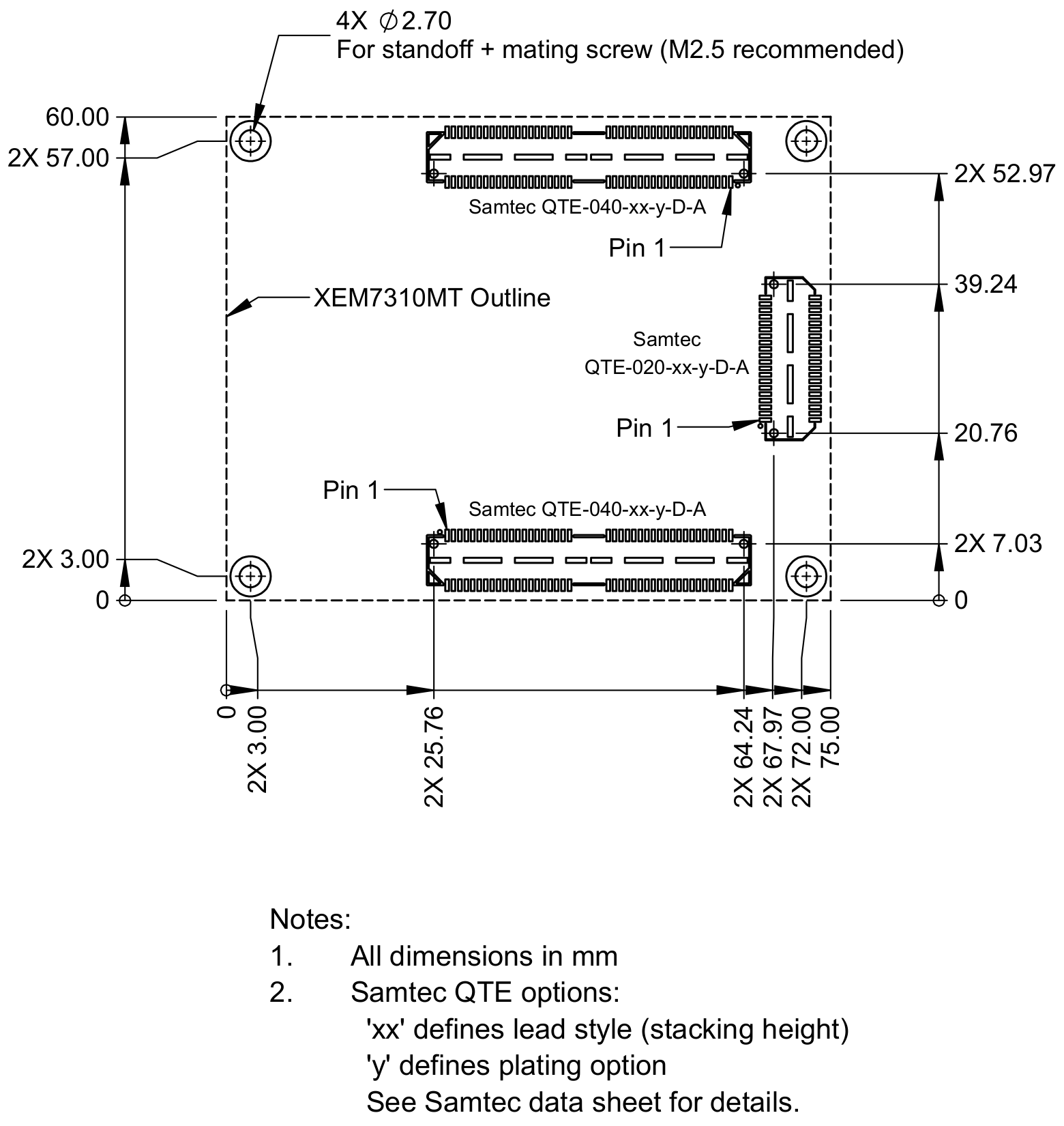
PCB Footprint
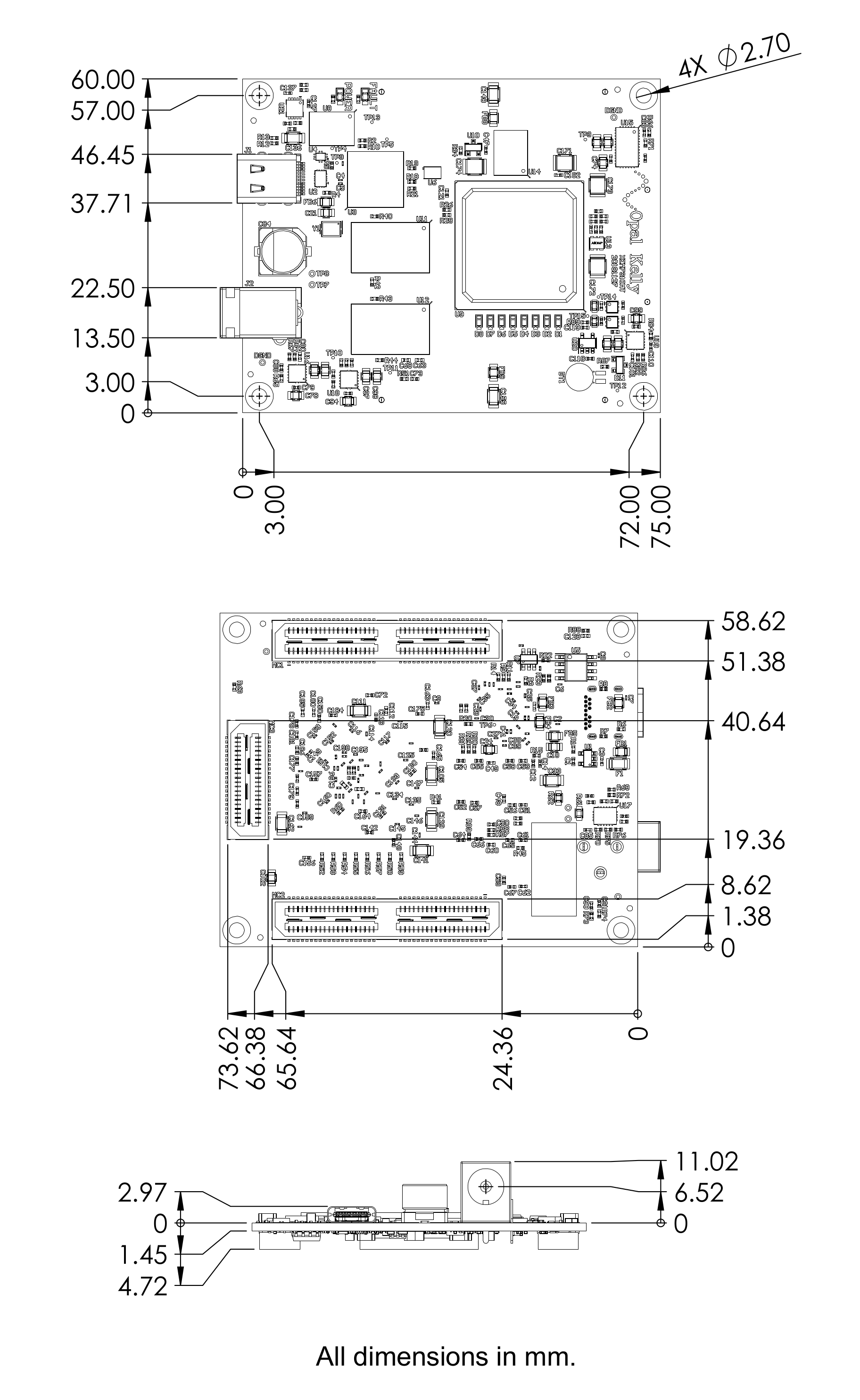
The XEM7310MT PCB is 75mm x 60mm with four mounting holes (M2.5 metric screws) spaced as shown in the drawings below. These mounting holes are electrically isolated from all signals on the XEM7310MT. The two connectors (USB and DC power) overhang the PCB edge slightly in order to accommodate mounting within an enclosure.
The XEM7310MT has two 80-pin and one 40-pin high-density Samtec connectors on the bottom side which provide access to many FPGA pins, power, JTAG, and transceivers.
Mechanical Drawing
The mechanical drawing below may be used for enclosure or mounting hardware design. 3D Models are also available in SolidWorks, STEP, and IGES formats.
Mating Board Diagram
Use the mating diagram below to orient and design peripheral mating hardware. Note that this is a top-down view and mates to the bottom of the XEM7310MT. This design is realized in Altium CAD drawings in the corresponding breakout board which are available through Pins Downloads.
For Samtec connector details, drawings, models, and landing patterns, please visit Samtec’s website.