XEM7320
JTAG and XADC
JTAG
The JTAG connections on the FPGA are wired directly to a dedicated 2×7 2mm header J2 compatible with the Xilinx JTAG cable and Digilent JTAG-HS3. The JTAG interface presented at J2 is a 1.8v interface corresponding to the FPGA JTAG I/O voltage.
XADC
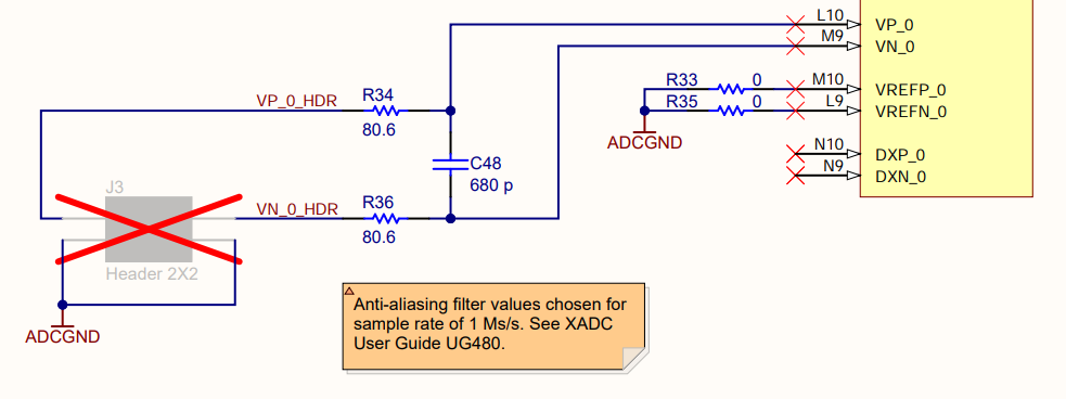
FPGA XADC signals are available on a dedicated, non-populated 4-pin header at J3. The ADC signals are filtered through a simple RC network.
The XADC uses the on-chip reference option which is selected by connecting VREFP and VREFN to
ADCGND.
Below we show the XADC connections to the Artix-7 Configuration bank: