Specifications
| Host Interface | USB 3.0 Type C, SuperSpeed FrontPanel Support |
| FPGA | XC7S50-1CSGA |
| Memory | 512 MiByte DDR3, 32-bit wide data interface |
| NV Memory | 16 MiB System Flash (15 MiB available for FPGA configuration boot or other storage) |
| Oscillator | 200 MHz |
| FPGA I/O Voltage | See Powering the XEM7305 |
| MINIMUM | TYPICAL | MAXIMUM | UNITS | |
|---|---|---|---|---|
| DC Input | +4.5 | +5.0 | +5.5 | VDC |
| DC Input Ripple | – | – | 50 | mVp-p |
| Operating Temperature | 0 | – | +70 | ºC |
| Storage Temperature | -50 | 0 | +100 | ºC |
| Weight | 15 | grams | ||
| Oscillator Frequency | 200 | MHz | ||
| Oscillator Freq. Stability | ±50 | ppm | ||
| Oscillator Period Jitter | 2.5 | ps RMS |
PCB Footprint
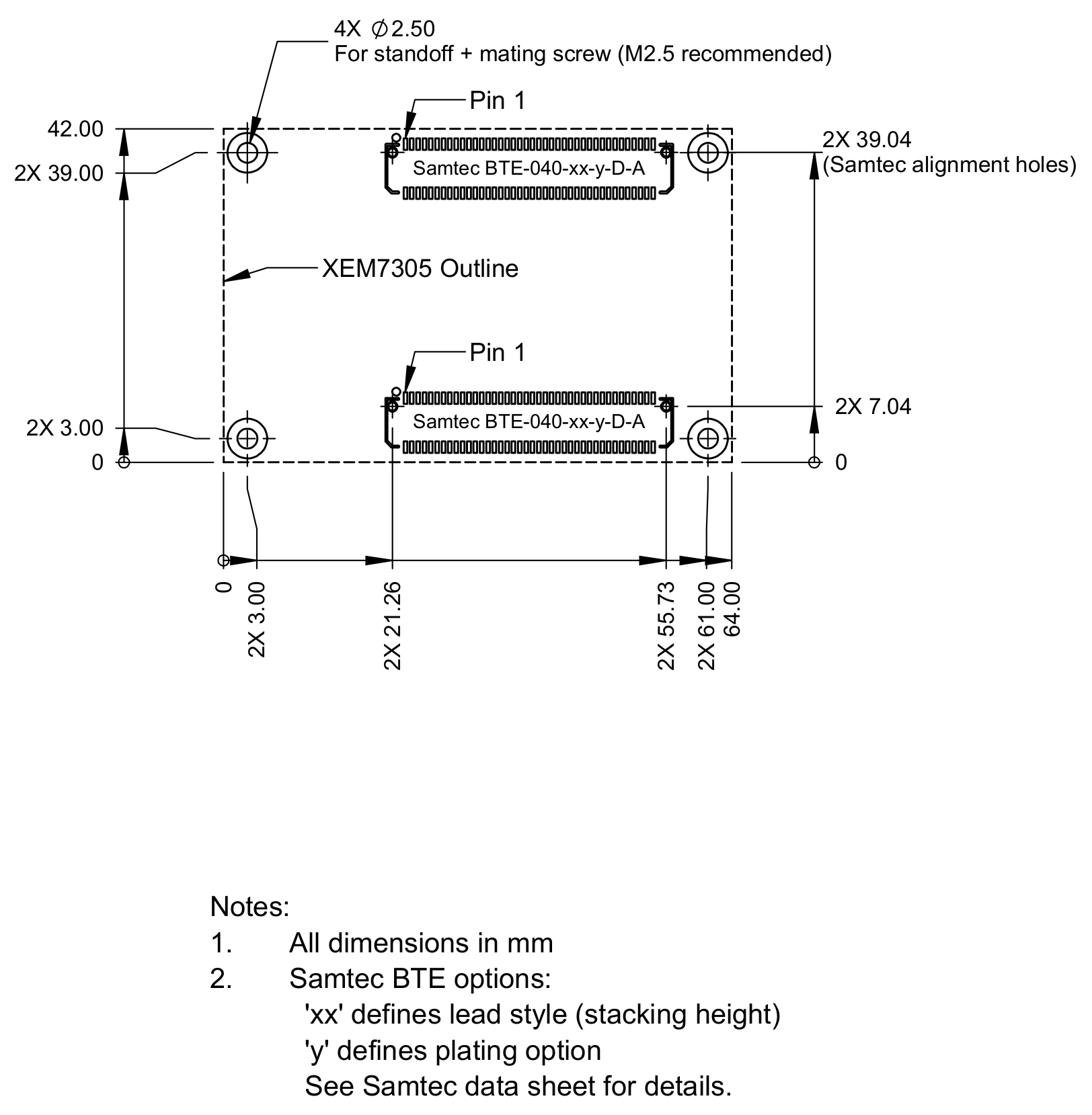
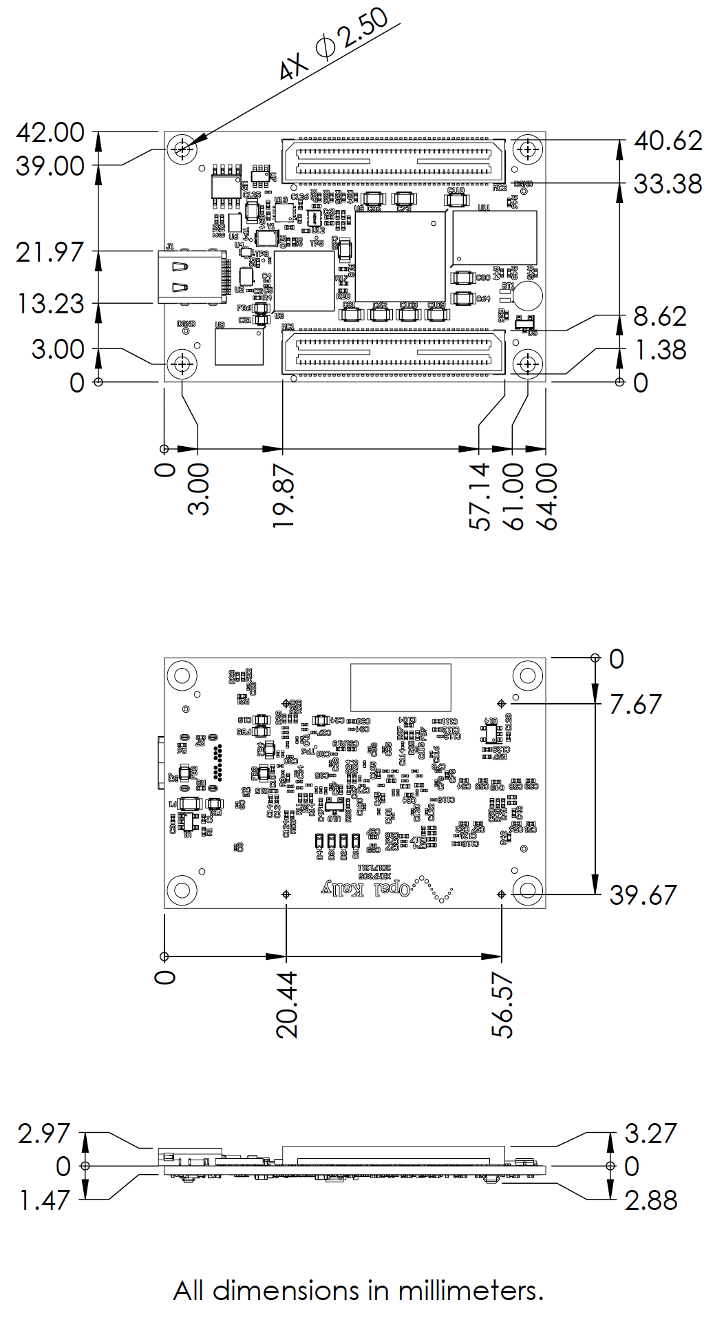
A mechanical drawing of the XEM7305 is available in PDF and image formats. The PCB is 64mm x 42mm (2.52″ x 1.65″) with four mounting holes (M2 metric screws) spaced as shown in the figure. These mounting holes are electrically isolated from all signals on the module.
The XEM7305 has a two 80-pin Samtec BSE connectors providing access to 108 I/O including 6 MRCC pins.
Mechanical Drawing
The mechanical drawing below may be used for enclosure or mounting hardware design. 3D Models are also available in SolidWorks, STEP, and IGES formats.
Mating Board Diagram
Use the mating diagram below to orient and design peripheral mating hardware. Note that this is a top-down view and mates to the top of the XEM7305. This design is realized in Altium CAD drawings in the corresponding breakout board which are available through Pins Downloads.
For Samtec connector details, drawings, models, and landing patterns, please visit Samtec’s website.