BRK7305 Breakout Board
The BRK7305 Breakout Board is a simple reference design intended to mate to the XEM7305 and provide easy, low-density access to the signals on the high-density mezzanine connectors on the XEM7305. The BRK7305 also provides necessary power supplies to the XEM7305 as well as a JTAG header compatible with the Xilinx Platform Cable USB.
Schematics and Layout
The BRK7305 schematic and layout are available as an Altium Designer project. If you use Altium Designer, you may start with this project as a way to build your own peripheral. Please visit our Pins Downloads page for additional information.
Power Supplies
| SUPPLY | VOLTAGE | MAX CURRENT | PART NUMBER | TYPE |
|---|---|---|---|---|
| +1.0VDD | 1.0 V | 2 A | Altera EN5322 | Switching |
| +1.5VDD | 1.5 V | 1 A | Texas Instruments TPS7A7100RGWT | Linear |
| +1.8VDD | 1.8 V | 1 A | Texas Instruments TPS7A7100RGWT | Linear |
| +3.3VDD | 3.3 V | 1 A | Texas Instruments TPS7A7100RGWT | Linear |
Switches
SW1 controls the PWR_EN (power enable) pin on all of the power supplies on the BRK7305. If you switch this to the off position, all supplies will be disabled.
SW2 selects the +VDC input voltage for all supplies on the BRK7305. In the +5VDC position, the power connector is the input source for all supplies. In the +5VUSB position, the USB power from the XEM7305 USB connector is used as the input source. Please refer to the Powering the XEM7305 page for more information on powering the XEM7305 through the USB connector.
SW3 controls the regulation voltage of U3, the linear regulator that establishes the DDR3 voltage. This can be used to set the voltage to 1.35 V (as used by DDR3L parts) or 1.5 V (as used on standard DDR3). The memory device on the XEM7305 will operate at either voltage.
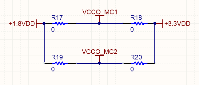
I/O Bank Power
The two I/O bank power supplies are configurable with 4 resistors located on the top layer of the PCB. You can selectively remove and populate these resistors to control the VCCO supplies for the I/O banks. If you need to set a value other than +1.8 V or +3.3 V for VCCIO, you can remove both resistors and apply the voltage externally.
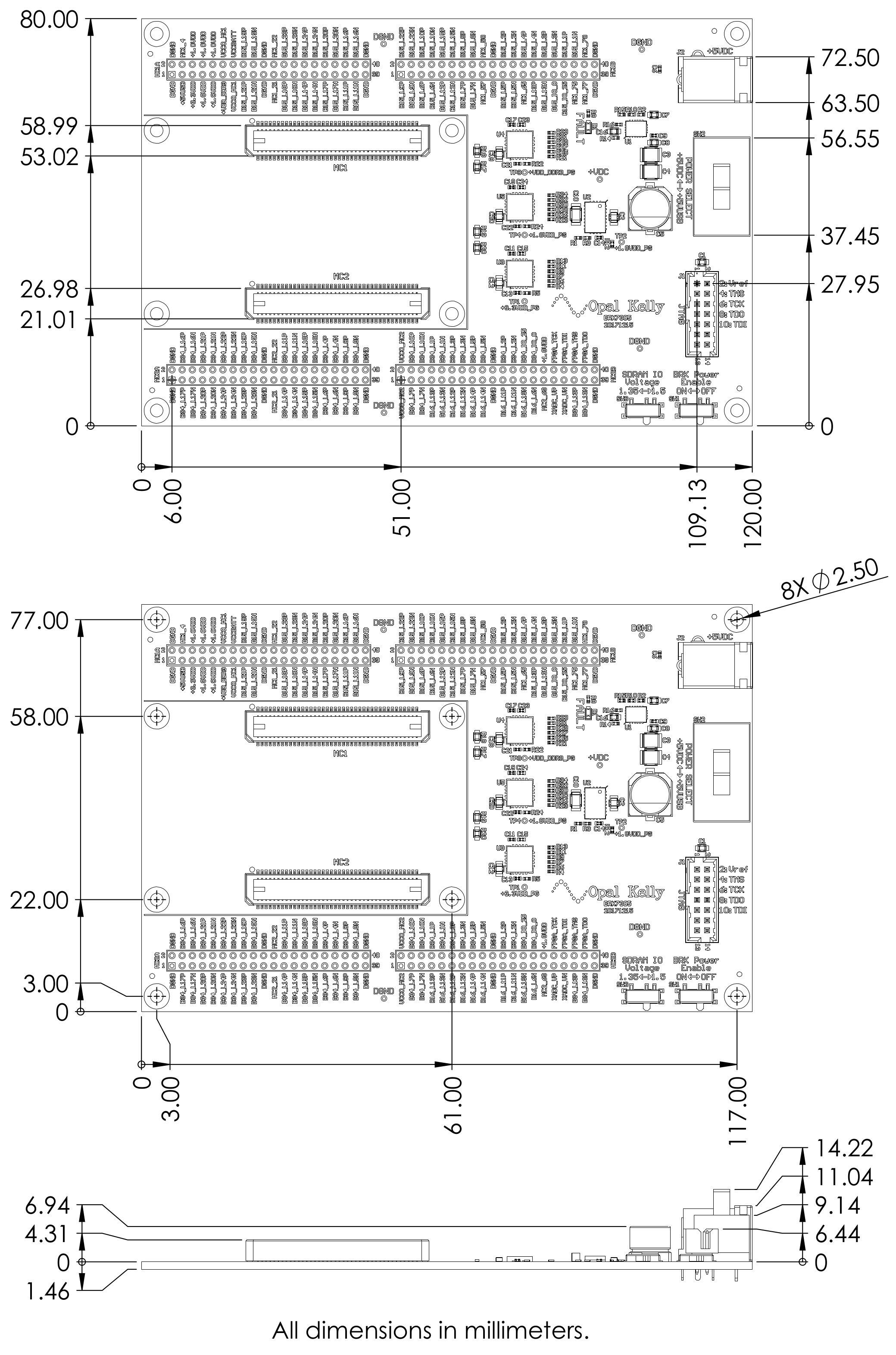
Mechanical Drawing