Leveraging Commercially-available, Off-the-shelf FPGA Boards and “Standard” Connectors to Build Semiconductor and Sensor Evaluation Platforms
Design engineers are generally an extremely busy and highly skeptical bunch. These characteristics present a challenge for any company fielding a new semiconductor device or sensor technology. Hounded by ever-shorter design cycles, ever-smaller development budgets, and the relentless march of technology, design engineers often look to evaluation boards to guide their component selection, for application guidance, and for proven design examples. The challenge for semiconductor or sensor companies is how to deliver a useful and affordable evaluation solution that also effectively demonstrates the unique capabilities of the underlying technology. Ideally, the design and development of such an evaluation solution could be leveraged and re-used across multiple platforms, markets, and application spaces.
As a semiconductor or sensor manufacturer, what are the options? Many vendors are seduced by the idea of a fully customized, proprietary design, which indeed may be the best solution for high production volumes or for applications targeting very specific solution domains. Unfortunately, fully customized solutions often carry extra development risk and cost but often offer little flexibility beyond the envisioned target application.
For most general-purpose semiconductor or sensor products, a better overall solution leverages a commercially-available off-the-shelf (COTS) board coupled with a small customized application card, as shown in Figure 1. The off-the-shelf content is typically an FPGA or microcontroller board with a widely-supported expansion connector (more about this later). The semiconductor or sensor vendor then creates a much simpler application daughter card that attaches via the “standard” connector. The smaller and simpler application card reduces development risk and lowers manufacturing costs. A Field-Programmable Gate Array (FPGA) provides a fully-programmable, flexible “gasket” to interface with the new device or sensor. FPGAs provide abundant, flexible I/O pins that support different I/O standards and voltages, including differential I/O standards like LVDS.
Sometimes, the entire demonstration application is self-contained to the FPGA or microcontroller board. However, oftentimes a graphical software interface makes the user experience more enticing and easy to use. However, connecting the physical hardware to the graphical software requires a communications interface with the host PC. The communications interface typically uses a widely-supported standard such as USB or Ethernet. Some off-the-shelf boards, like those from Opal Kelly, also provide the necessary software drivers and programming language infrastructure to support more advanced application development, which saves the hassle and expense of creating and maintaining a proprietary set of drivers.
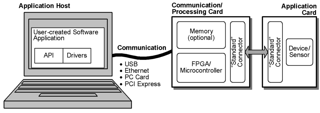
Figure 1: An example total solution for creating an evaluation platform for a new device
The remainder of the article explores various solutions and discusses the advantages and disadvantages of various options.
Connectors
Leveraging off-the-shelf board solutions, the semiconductor or sensor vendor produces a small, simple application card that features the company’s “secret sauce” technology. There is a popular set of options to connect the application daughter card to the base communications/processing card shown in Figure 1. The choice of connector is dictated by the communications and bandwidth requirements of the attached semiconductor or sensor application and by the availability of support hardware or software. Table 1 lists some of the “standard” connectors more commonly found on FPGA and some processor boards.
Table 1: Widely-supported “Standard” Connectors
| Format | Best for … | Connector | Version | Maximum Digital I/O | Maximum Differential I/O Pairs | Maximum Gigabit Transceiver Channels |
|---|---|---|---|---|---|---|
| Pmod™ Peripheral Modules | Simple, low I/O-count applications with low bandwidth requirements | 1×6 0.1” header | Pmod6 | 4 | Not defined | 0 |
| 2×6 0.1” header | Pmod12 | 8 | Not defined | 0 | ||
| Two 2×6 0.1” headers | Double Pmod12 | 16 | Not defined | 0 | ||
| FMC (ANSI/VITA 57.1) | High I/O, high bandwidth applications | One LPC SEARAY socket | Low Pin-Count (LPC) | 68 | 34 | 1 |
| One HPC SEARAY socket | High Pin-Count (HPC) | 160 | 80 | 10 | ||
| Two HPC SEARAY sockets | Double-wide HPC | 320 | 160 | 20 |
Pmod Peripheral Modules: Low Pin Count, Moderate Bandwidth
- Low cost
- Easy to manufacture
- Ideal for applications with few I/O and moderate performance requirements
- Easy board-to-board cabling
Low pin count and low- to moderate-bandwidth applications fortunately also require a simple, low-cost connector. Many semiconductor devices and sensors communicate using simple serial interfaces such as four-wire SPI or JTAG, two-wire interfaces such as I2C, I2S, or CAN, or even one-wire interfaces such a 1Wire. An SPI interface, for example, requires just six pins—four signals, power, and ground. One widely supported “standard” in this arena is the Digilent Peripheral Module (Pmod) connector, found on a variety of FPGA and microcontroller boards offered by numerous vendors. As shown in Figure 2, there are three variants of the Pmod interface.

Figure 2: Three Variants of Peripheral Module (Pmod) Connectors
In its simplest form, a Pmod connector is simply four wires, power, and ground. The connector is just six stake pins or holes on 0.1” (2.54 mm) pitch or a comparable female mating socket. Power is either selectable between +5V and +3.3V, or a constant +3.3V. Some FPGA boards provide additional flexibility by supporting other supply voltages, although not all off-the-shelf Pmod modules support this. The I/O pins on FPGAs generally support a variety of voltage standards—a feature not common on microcontrollers.
A Pmod connector supports switching up to about 50 MHz per pin, or about 20 MHz over a cable. Application or daughter cards that plug directly into the host board should be 0.8” wide or less, although larger boards are easily accommodated via cabling.
The next step up in bandwidth a 12-pin Pmod socket—a 2×6 array of holes or pins. Figure 3 shows an example daughter card using the 12-pin Pmod option. The 12-pin Pmod variant offers 8 I/O connections, two power connections, and two ground connections. Alternatively, a 12-pin Pmod connector also functions as two independent 6-pin Pmod sockets as shown in Figure 4.
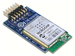
Figure 3: Example 12-pin Pmod module; an 802.11b WiFi Interface
Finally, a double-wide 12-pin Pmod format provides up to 16 I/O connections. Essentially, this format is two 12-pin Pmod sockets spaced 0.9” inches apart as shown in Figure 4. A double-wide application daughter card uses two adjacent 12-pin Pmod sockets, which together provide 16 I/O connections, four power connections, and four ground connections. A double-wide socket also performs as two independent 12-pin Pmod sockets or four independent 6-pin Pmod sockets.
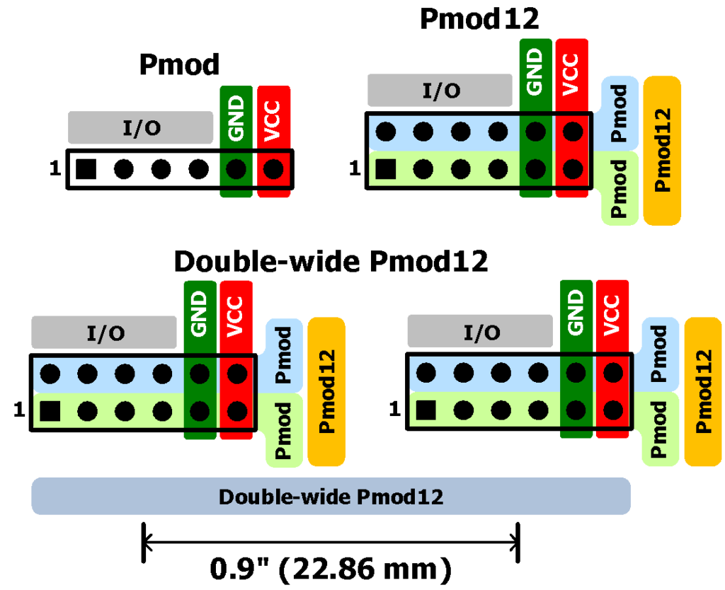
Figure 4: Examples of the 6-pin, 12-pin, and Double 12-pin Pmod Interfaces
Table 2 lists the various suppliers offering host boards and application daughter cards that support the Pmod standard.
Table 2: Vendors Offering Pmod-Compatible Hardware Solutions
| Host Board Providers | Application Daughter Cards |
|---|---|
| Avnet | Analog Devices |
| Digilent Inc. | Avnet |
| Lattice Semiconductor | Digilent, Inc. |
| Opal Kelly Incorporated | Maxim |
| Xilinx | Microchip |
For additional information on the Pmod “standard”, visit the Digilent web site.
Pmod Peripheral Module Interface Specification
www.digilentinc.com/Pmods/Digilent-Pmod_%20Interface_Specification.pdf
Pmod Licensing
www.digilentinc.com/Pmods/licensing.cfm
FPGA Mezzanine Card (FMC) (ANSI/VITA 57.1): High Pin Count, High Bandwidth
- Widely supported, industry-standard interface
- High I/O, up to 160 digital I/O and ten gigabit transceiver lanes
- Compact connector with excellent signal integrity
- Two electrically- and mechanically-compatible connector variants
- Supports multiple I/O standards and voltages
The FPGA Mezzanine Card (FMC) standard provides solutions that support the most total I/O and highest bandwidth—including potentially up to ten channels of multi-gigabit serial data. As an official industry standard (ANSI/VITA 57.1), FMC offers wider interoperability and broader support by a range of vendors. FMC-based cards come in two basic flavors but use a nearly identical, mechanically- and electrically-compatible connector measuring just 56.62 mm by 13.23 mm. Figure 5 shows the male and female connectors for the Low Pin-Count option. The maximal I/O option, called High Pin-Count or HPC, uses a 400 connection (40×10 array) high-density socket with excellent signal integrity, as shown in Figure 6a. A subset, called Low Pin-Count or LPC, has 160 connections but remains mechanically and electrically compatible with HPC sockets, as shown in Figure 6b. LPC cards operate in HPC sockets and the LPC subset of HPC mezzanine cards operate in an LPC socket. This flexibility allows an FMC add-on or mezzanine card to be easily retargeted to new FMC base boards.
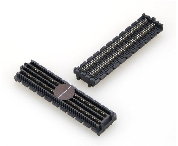
Figure 5: Male and female Low Pin-Count (LPC) connectors
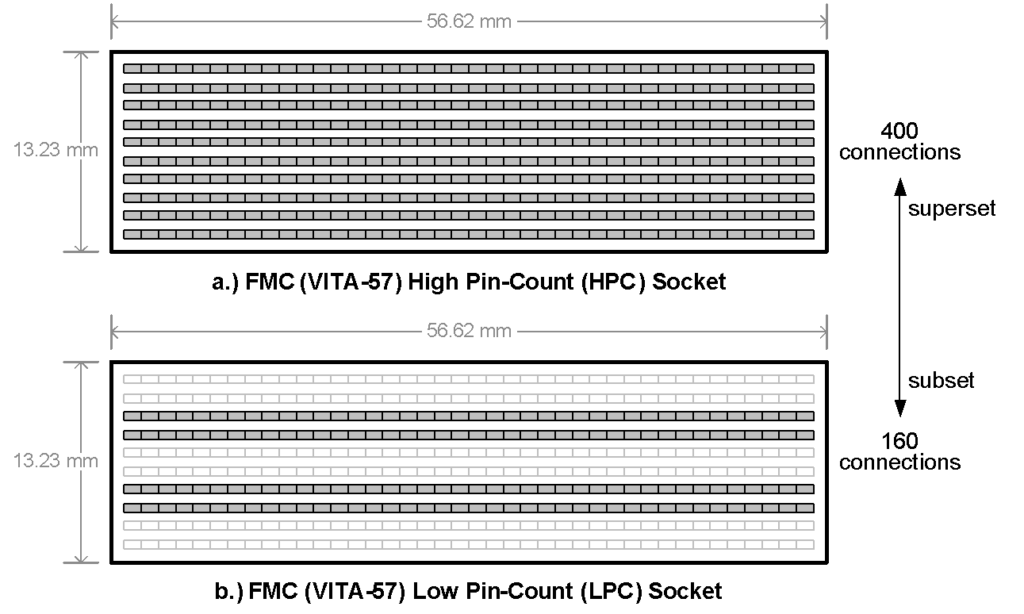
Figure 6: FPGA Mezzanine Card connectors come in two flavors: High Pin-Count (HPC) and Low Pin-Count (LPC)
An FMC carrier card (the motherboard or base board) uses a female connector while mezzanine cards (application daughter cards) use a male connector. FMC also supports a double-wide option, providing even more total I/O connections.
For optimal signal integrity, the FMC socket provides copious amounts of ground connections and provides physical separation of high-speed differential I/O and clock signals.
Low Pin-Count (LPC) Mezzanine Card
- Uses a 160-connection LPC connector (see Figure 5 and Figure 6b)
- Up to 68 digital I/O signals or 34 differential I/O signals on a single I/O bank supply (see Figure 7a)
- Definable I/O voltage standard
- Voltage is defined in an I2C-standard, IMPI-standard personality PROM located on the mezzanine card
- FMC carrier reads the I2C-standard personality PROM and sets the I/O voltage supply (0V to 3.3V)
- Up to two LVDS reference clocks provided by the mezzanine card
- Supports up to one gigabit transceiver lane (transmit lane plus receive lane), including a reference clock lane
- Includes JTAG IEEE 1149.1 signaling
- Receives 3.3V and optionally 12V power from the carrier card for powering components and for efficiently generating other necessary voltage levels on the mezzanine card
High Pin-Count (HPC) Mezzanine Card
- Uses a 400-connection HPC connector (see Figure 6a)
- Supports every function of an LPC mezzanine card plus additional capabilities
- Adds another 48 digital I/O signals or 24 differential I/O signals to I/O Bank A plus bolsters the I/O Bank A supply input
- Provides a second I/O bank (I/O Bank B)
- Supports up to 44 digital I/O signals or 22 differential I/O signals
- I/O voltage optionally provided by the mezzanine card, although may use the same voltage supply as I/O bank A
- Provides two additional LVDS clock connections
- Clocks can optionally be provided by the carrier or the mezzanine card
- Direction of the clock connections are controlled by an input from the mezzanine card
- Provides up to nine additional gigabit transmit and receive lanes (transmit lane plus receive lane) plus an additional reference clock lane
- Adds more total ground connections and provides isolation for the high-speed differential I/O channels
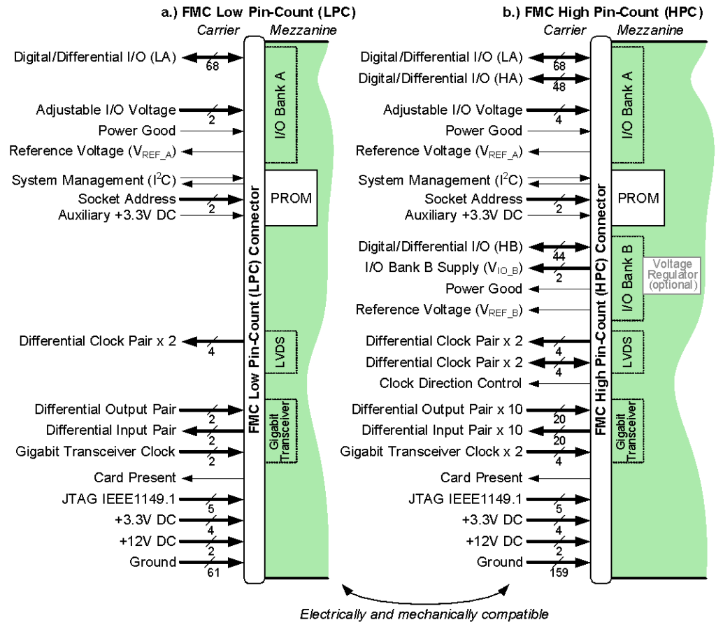
Figure 7: The Low Pin-Count (LPC) and High Pin-Count (HPC) FMC connectors are electrically and mechanically compatible
The FMC specification also provides a double-wide option that doubles the board area for the mezzanine card and optionally doubles total I/O available.
FMC-based carrier and mezzanine cards are available from a variety of suppliers, ranging from simple single-FPGA designs to multi-FPGA boards that deploy the latest and largest FPGAs. FMC-basic carrier cards are also available in different industry-standard form factors including VME, VPX, CompactPCI, AdvancedTCA, MicroTCA, PCI, PXI, and many other low profile formats.
Visit the FMC Marketing Alliance web site (www.vita.com/fmc.html) for a partial list of suppliers. The official FMC/VITA-57.1 specification is also available for purchase from the web site.
Samtec SEARAY™ FMC LPC and HPC Connectors
Samtec FMC flex cables
Virtual I/O, Configuration, and Software Support
The base board and adapter card likely contain a variety of input and output devices. Adding more or different I/O can be expensive, especially to support new functionality after completing the design and assembly. However, by connecting the entire application to a PC, the PC itself can provide a rich set of “virtual” I/O functions. PC connectivity also enables custom software applications that interact directly with the application hardware and can leverage the PC’s physical interfaces. For example, most PCs are connected to the Internet, facilitating remote software updates and downloads of new features and functions.
Four items are required to create a usable virtual I/O environment.
- A communications mechanism between the hardware and a PC or workstation.
- Program or configure the underlying hardware
- Send and receive (read and write) data to and from the hardware
- A communications interface software driver for the PC or laptop, available for various operating systems.
- VHDL and Verilog source files to create the necessary hardware interface inside the FPGA.
- Support packages for various software programming languages such as C, C++, Java, and Python. DLLs to support other environments such as Matlab and LabVIEW.
Table 3: Available Software Support
| Opal Kelly FrontPanel | |
|---|---|
| Operating System Support | Windows x32 and x64Linux (x36 and x64)OS XQNX Neutrino |
| Software Development Kit available? | Yes |
| Communications Drivers | USB, PCI Express |
| FPGA-side interface logic | VHDLVerilog |
| Language Support | CC++C#JavaPythonDLL support |
| Virtual components | LEDsHexadecimal displaysSlidersPushbuttonsCheck boxesToggle buttonsNumerical entry |
Some base-board vendors provide additional software and pre-built applications to create “virtual” I/O connections, such as Opal Kelly’s FrontPanel environment showcased in Table 3. The FrontPanel environment provides a library of simple virtual I/O components as shown in Figure 8. These virtual components include work-alike equivalents for physical pushbutton or slide switches and physical LEDs and 7-segment displays. The components also include software elements like control buttons, graphical check boxes, and text display boxes. Using the virtual I/Os, an engineer can conveniently control and monitor functions located on the application daughter card, all from the comfort and convenience of his or her PC. Essentially, the software running on the PC communicates to the FPGA on the base board, typically over USB. The FPGA provides the programmable interface “gasket” between the USB controller on the base board and the specialized function located on the application card, as shown in Figure 1.
The FrontPanel application example shown in Figure 8 controls and communicates with various Pmod add-on peripheral modules attached to an Opal Kelly XEM6002 board. Connected to the board are Pmod modules with …
The FrontPanel graphical interface also controls and monitors registers within an 8-bit PicoBlaze controller implemented within the FPGA on the XEM6002 board. With the FrontPanel widget set, the I/O connections to the board can appear as physical switched and LEDs or as graphical elements within a standard software user interface.
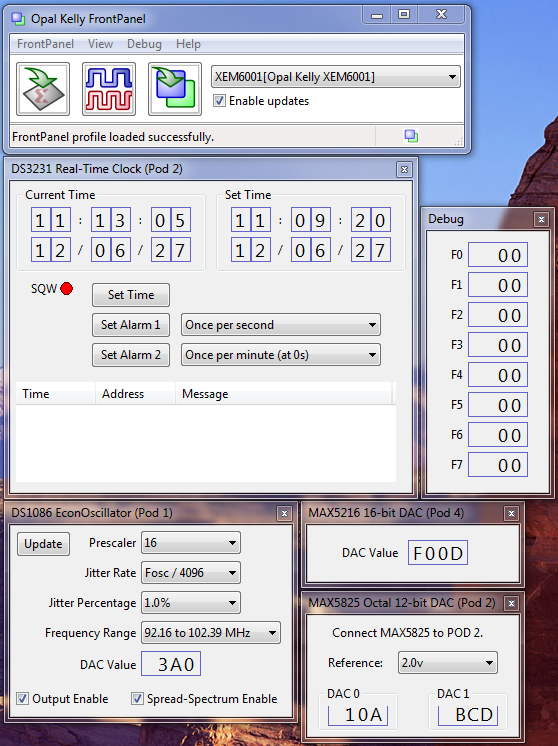
Figure 8: Opal Kelly FrontPanel Application Controlling Multiple Pmod Modules and PicoBlaze Microcontroller Implemented in the FPGA
The available FrontPanel software provides pre-built virtual I/O components. However, the range of possible virtual I/O components is limited only by the imagination of the programmer. The Opal Kelly Front Panel package provides the necessary hooks to popular programming languages such as C, C++, C#, Java, and Python. Figure 9 shows an example of a custom C++ application built using the FrontPanel application to display the image captured by an attached 5 Mexapixel CMOS image sensor, shown in Figure 10.
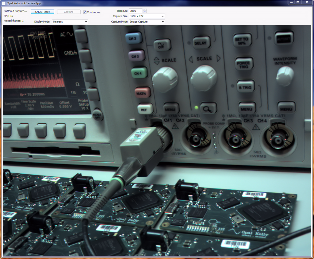
Figure 9: CMOS Image Sensor Connected Opal Kelly Shuttle LX1 Board, Displayed on PC Display via USB Connection
Figure 10 shows the physical hardware connected to the PC application. The base board in this application is an Opal Kelly Shuttle LX1 board, which includes a Low Pin-Count (LPC) FMC connector. The Shuttle LX1 board is the industry’s smallest and least expensive FMC carrier cards (base boards). The Shuttle LX1 board is about the size of a credit card and includes a high-speed USB 2.0 controller, a Xilinx Spartan-6 FPGA, and 128 Megabytes of DDR2 SDRAM, as shown in Figure 12. The Shuttle LX1 includes all the necessary functions required for an FMC carrier card but without the expensive “bells and whistles” extra features of some carrier cards.
The CMOS image sensor is an Opal Kelly EVB1006 FMC mezzanine card that plugs directly into the Shuttle LX1 board.
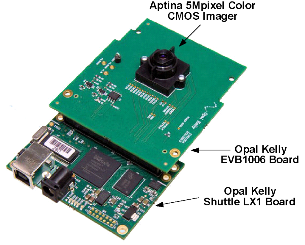
Figure 10: Opal Kelly Shuttle LX1 Board with 5Mpixel Color CMOS Imager Card
The CMOS image sensor captures data at too fast a data rate to control and receive directly from the host PC. Instead, control and data capture operations are off-loaded to the FPGA on the Shuttle LX1 card. The FPGA captures data from the image sensor in RGGB Bayer pattern format, shown in Figure 11a, and converts the image to standard RGB format for the host application running on PC, shown in Figure 11b. The image conversion algorithm leverages the parallel processing capabilities of the FPGA on the Shuttle LX1 card and also uses the 64Mx16 DDR2 SDRAM memory.

Figure 11: The 5Mpixel CMOS imager uses a different pixel pattern than traditional PC displays
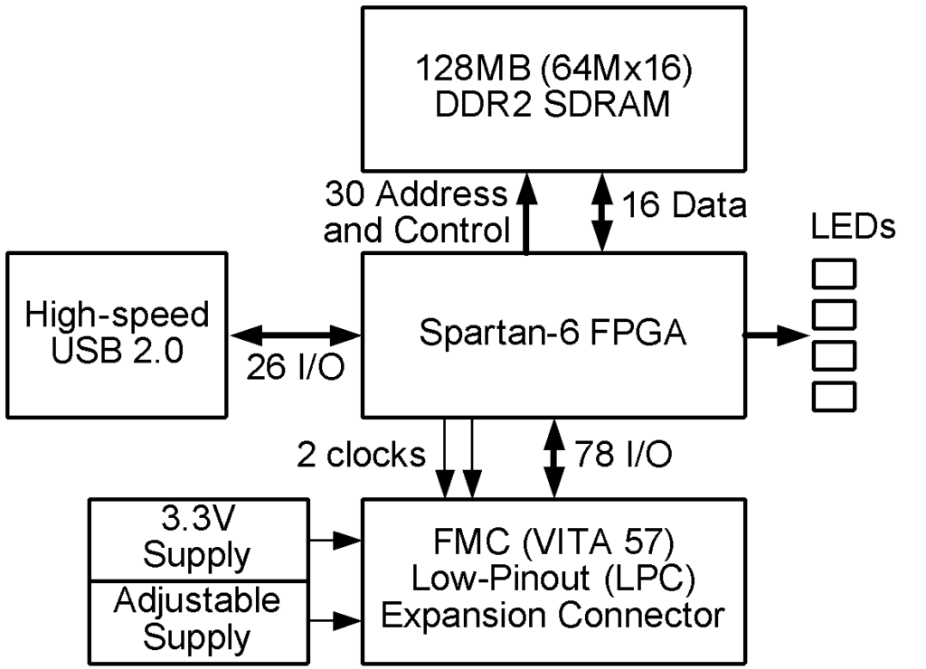
Figure 12: Architecture of the Opal Kelly Shuttle LX1 Card
The camera and FPGA are controlled via the custom-built C++ application running on the host PC. The image data is captured by the Shuttle LX1 card and displayed on the PC’s graphical display via the custom software application. The Shuttle LX1 includes a high-speed (HS) USB 2.0 interface to the PC that provides up to 36 Mbytes per second of bandwidth. This bandwidth allows the PC to display real-time HD-like images (1296×972) at 21 frames per second using 24-bit color per pixel. At maximum resolution (5Mpixels or 2592×1944), the application can display 7 frames per second at 24 bits per pixel.
Opal Kelly Shuttle LX1 FMC Carrier Card
www.opalkelly.com/products/xem6006/
Opal Kelly EVB1006 5-Megapixel CMOS Image Sensor for Shuttle LX1
www.opalkelly.com/products/evb1005/
The Opal Kelly FrontPanel environment also includes a DLL driver and a Applications Programming Interface (API). The DLL driver and API allows the application hardware to be integrated into other software environments such as Mathworks MATLAB and National Instruments LabVIEW.
For example, Figure 13 shows a screen capture of a LabVIEW application built to communicate with a Texas Instruments (TI) AD1675 Reference Design board, which demonstrates a 4MSPS, high-speed, high-precision, 24-bit analog-to-digital converter (ADC). The analog daughter card and the PC communicate via an Opal Kelly XEM3010 board that uses a proprietary connector between the base board and the application daughter card.
From the host PC, an engineer evaluating the AD1675 ADC converter can capture and view actual signals from the converter card using a compiled LabVIEW application. The LabVIEW application—running ot the PC host—transmits configuration parameters to the ADC converter and triggers capture operations via the USB interface 2.0. The Opal Kelly card captures the data from the converter, formats it, and optionally provides some hardware-based pre-processing. Ultimately, the captured data is transmitted back to the host PC for viewing and analysis. The LabVIEW software application provides sophisticated virtual I/O functions such as a multichannel FFT analyzer.
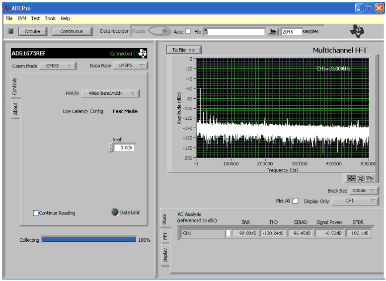
Figure 13: LabVIEW Connected to Texas Instruments’ ADS1675 Reference Design via Opal Kelly Card
For additional information on this application example, see the ADS1675REF User’s Guide on the Texas Instruments web site.
ADS1675REF User’s Guide
http://www.ti.com/lit/ug/sbau162a/sbau162a.pdf
Lastly, the PC communications interface also provides services to download and configure the FPGA and sometimes to program Flash memory on the base card or daughter card.
Communication
Just as there are options for selecting a connector interface, there are options for selecting a communications mechanism between the host PC and the target application, as listed in Table 4. RS-232 serial communication has been a mainstay in the semiconductor world but it is low bandwidth and no longer widely supported on modern PCs. RS-232 is quickly being replaced by ubiquitous USB. USB itself comes in multiple flavors. USB 1.0 is sufficient for low-bandwidth applications but USB 2.0 support is now widespread and offers far superior performance. USB 3.0 deployment is just beginning but it offers enticingly high bandwidth.
1G and 10G Ethernet offers high bandwidth as does PCI Express. However, neither offers the general ease-of-use of USB. However, until USB 3.0 support become more widespread, only 10G Ethernet and PCI Express offer very high bandwidth.
Table 4: Potential communication methods between the host PC and target application card
| Communication Method | Pro | Con |
|---|---|---|
| RS-232 | Simple, proven. | Obsolete on modern PCs. May require separate adapter. Limited bandwidth |
| BlueTooth | Good for low bandwidth | |
| USB 1.0 | Widely supported. Ubiquitous. | Supports only moderate data rates |
| USB 2.0 | Widely supported. Ubiquitous. High bandwidth (about 35 Mbytes per second) | Supports up to about 35 Mbytes per second |
| USB 3.0 | Very high bandwidth, up to 300 Mbytes per second | Emerging standard. Only available in newer systems. Driver support is limited. |
| Ethernet | High to very-high bandwidth | Lack of power supply |
| WiFi | Wireless | Can be difficult to connect in some systems. Limited bandwidth depending on variant. |
| PC Card | High bandwidth. | Restrictive card size. Not available in all systems. |
| PCI Express | Very high to extreme bandwidth | No commonly-available connector. Likely requires a separate adapter card. |
Make vs. Buy Decisions
For many semiconductor device and sensor vendors, the primary decision is, do you …
- Design your own fully-custom evaluation board, including software driver support, or
- Design an application daughter card that plugs into a commercial off-the-shelf (COTS) base board, such as those offered by Opal Kelly.
Table 5 summarizes various aspects of the “make vs. buy” decision, including some of the trade-offs.
Table 5: Trade-offs of the “Make vs. Buy” decision.
| Fully-custom Design | Off-the-shelf Opal Kelly Base Board Plus Custom Daughter Card | |
|---|---|---|
| Best application type | Very high production volume or specific, tightly-targeted application | General-purpose applications. Flexibility for new markets and applications. |
| Design base board | Include both base and application design on a single card. About 6-7 months of total development time ($70,000) | Purchase commercially-available off-the-shelf (COTS) board |
| Flexibility, ease of moving to new markets and opportunities | Typically not re-useable for new markets or opportunities | Application daughter card can be re-used and repurposed on other base boards using the same connector |
| Design application daughter card | Tied to base board. No future flexibility. | Greatly-reduced design effort. About 1-2 months of development time ($20,000) |
| Write device driver for communications interface | Possibly included by the vendor of the communications device | Included in FrontPanel environment |
| Virtual I/O library | Custom development, including both software and on-board logic design | Included in FrontPanel environment |
| 675\Add support for programming languages | Requires additional development cost per language | Included in FrontPanel environment |
| Support multiple operating systems for deployment | Requires additional development cost per operating system | Included in FrontPanel environment |
Conclusion
Commercially-available, off-the-shelf (COTS) FPGA or microntroller boards enable cost-effective demonstration and evaluation platforms for new semiconductor devices or sensors. FPGA board offer flexible interface, significantly higher I/O counts, and support multiple I/O and voltage standards. Instead of the cost, delay, and risk of a fully-custom design, a two-board solution provides more flexibility, lower risk, lower development cost, and typically, a better overall end-user experience. The daughter card containing the semiconductor device or sensor can be re-used on other base boards or even in customer applications if it uses a “standard” connector.
Some board vendors, like Opal Kelly, provide a rich set of support libraries, including device drivers and board support packages for programming languages like C, C++, and Java. These support packages enable easy-to-use graphical interfaces so that a design engineer can quickly and easily evaluate the semiconductor device or sensor.
Parking Lot (Material that may be used later)