Expansion Connectors
| Opal Kelly Pins is an interactive online reference for the expansion connectors on all Opal Kelly FPGA integration modules. It provides additional information on pin capabilities, pin characteristics, and PCB routing. Pins can also generate constraint files (XDC) and help you map your HDL net names to FPGA pin locations automatically. The Pins reference for the XEM8305 may be found at the link to the right. | XEM8305 Pins Reference Pins Documentation |
Connector Details
Three high-density connectors are available on the bottom-side of the XEM8305 PCB. These expansion connectors provide user access to several power rails on the XEM8305, the JTAG and SYSMON interfaces on the FPGA, 124 I/O pins, and access to the GTH transceiver banks.
The table below lists the Samtec connector part numbers as well as the mating connector and total mated height:
| Expansion Connector | Pins | XEM8305 PART NUMBER | Mating Connector | MATED HEIGHT |
|---|---|---|---|---|
| MC1 | 100 | ERM6-50-01.5-L-DV-A-K-TR | ERF6-50-03.5-L-DV-A-K-TR | 5.00mm (0.197”) |
| MC2 | 80 | ERM6-40-01.5-L-DV-A-K-TR | ERF6-40-03.5-L-DV-A-K-TR | 5.00mm (0.197”) |
| MC3 | 80 | ERM6-40-01.5-L-DV-A-K-TR | ERF6-40-03.5-L-DV-A-K-TR | 5.00mm (0.197”) |
MC1
MC1 is an 100-pin high-density connector providing access to FPGA Banks 64 (HP) and 84 (HD). VCCO_64 and VCCO_84 connections are also available on this connector. An external rail must be provided on the carrier board to power these I/O banks. See the External I/O Voltage section for more details.
DC input power must be connected to MC1 to supply power to the XEM8305.
Pin mappings for MC1 are listed on the pins page. See the Considerations for Differential Signals section below for information on expansion signal routing.
MC2
MC2 is an 80-pin high-density connector providing access to FPGA Banks 85 (HD), 86 (HD). VCCO_85 and VCCO_86 connections are also available on this connector. External power rails must be provided on the carrier board for these I/O banks. See the External I/O Voltage section for more details.
JTAG and XADC connections are also available on MC2.
Pin mappings for MC2 are listed on the pins page. See the Considerations for Differential Signals section below for information on expansion signal routing.
MC3
MC3 is an 80-pin high-speed connector providing access to GTH transceiver banks 224, 225, and 226. This includes connections to MGTREFCLK0 (224) and MGTREFCLK0 (225). The MGTREFCLK0 (226) connection is available on MC2.
The provided REFCLK pins have on board AC coupling capacitors while the transceiver lanes are directly connected to MC3.
Pin mappings for MC3 are listed on the pins page. See the Considerations for Differential Signals section below for information on expansion signal routing.
FPGA Bank Connections
| FPGA BANK | HR / HP | VOLTAGE RANGE | MCX | Power Rail | VREF | I/O AVAILABLE |
|---|---|---|---|---|---|---|
| 64 | HP | 0.95 – 1.90 V | MC1 | VCCO_64 | VREF_64 | 52* (including 4 GC pairs) |
| 84 | HD | 1.14 – 3.40 V | MC1 | VCCO_84 | N/A | 24 (including 4 GC pairs) |
| 85 | HD | 1.14 – 3.40 V | MC2 | VCCO_85 | N/A | 24 (including 4 GC pairs) |
| 86 | HD | 1.14 – 3.40 V | MC2 | VCCO_86 | N/A | 24 (including 4 GC pairs) |
* – Note: One bank 64 I/O pin is used for a VRP resistor by default. The resistor can be moved to connect the I/O pin to MC1 instead. See the VRP information below for details.
Setting the Expansion Connector I/O Voltages
The Artix UltraScale+ FPGA allows users to set I/O bank voltages in order to support several different I/O signal standards. External power rails must be provided on the carrier board for these I/O banks. See the External I/O Voltage section for more details.
Power
The expansion connectors are use to provide power to the XEM8305, as well as providing the carrier board assess to on board regulators. These power pins are listed on the Pins sheet. Further power details can be found on the Powering the XEM8305 page.
Power Good
The XEM8305 provides a power good signal on the expansion connector MC1 to signal that all on board power rails are up and good. The XEM8305_PG signal can be used to sequence the power on of external VCCO I/O regulators. FPGA power is good when this signal is high with a 1.8V signal level.
Clock Input Pins
Available global clock input fabric pins are shown in the XEM8305 Pins Reference. You can use the filter options to display these pins.
MGT Refclock 0 inputs are available on the expansion connector for all 3 transceiver quads (224, 225 and 226).
JTAG
The JTAG connections on the FPGA are wired directly to the expansion connector MC2 with 4.7kΩ pull-up resistors on TDI, TCK and TMS. The JTAG signal voltage is 1.8V. An appropriate connector (such as a 2mm connector compatible with the JTAG cable) is need on the attached carrier to the XEM8305. Our BRK8305 has this connector and may be used as a reference.
| JTAG CONNECTION | MC2 PIN | FPGA PIN |
|---|---|---|
TDO | 7 | Y10 |
TDI | 3 | AB12 |
TCK | 1 | AE12 |
TMS | 5 | AB10 |
SYSMON
FPGA system monitor signals are are wired directly to the expansion connector MC2.
VREFP may optionally provide a precision reference for optimal performance of the ADC. See UG580 UltraScale Architecture System Monitor for additional details.
By default, C168 is populated with a 0.1-μF decoupling capacitor so that an external voltage reference may be used. To enable the internal reference instead, the carrier board must short VREFP (MC2 pin 14) to GNDADC (MC2 pin 16). Alternatively, C168 could be replace with a 0-Ω 0402 resistor.
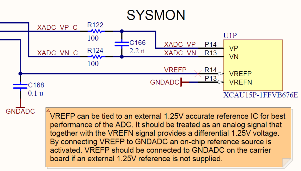
| MC2 PIN | FPGA PIN | CONNECTION |
|---|---|---|
| 14 | R14 | VREFP |
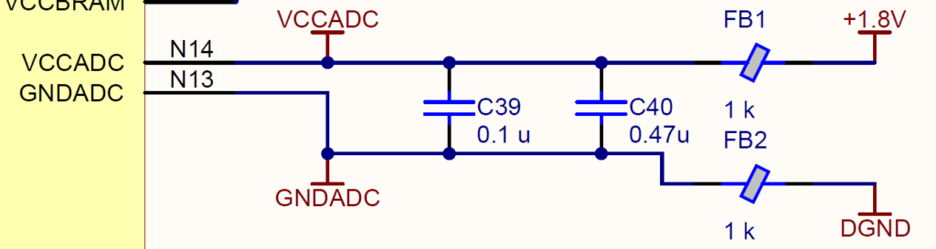
| 18 | N14 | VCCADC (1.8V supplied by the XEM8305 via FB1) |
| 16 | N13 | GNDADC (Connected to DGND via FB2) |
VREFN (FPGA P13) is connected directly to GNDADC.
XADC
The Artix UltraScale+ XADC feature is routed through two 100Ω resistors to the MC2 connector. There is a 2.2 n capacitor installed across the two FPGA pins for decoupling.
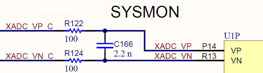
| MC2 PIN | FPGA PIN | CONNECTION |
|---|---|---|
| 12 | P14 | XADC_VP_C |
| 10 | R13 | XADC_VN_C |
VBATT
By default the VBATT functionality is disabled by the 0-Ω resistor R2 connecting it to ground. If it is required in your design, R2 must be removed. Then VBATT can be accessed on MC1.
Reference Voltage Pins (Vref)
The Artix UltraScale+ supports both internal and externally-applied input voltage thresholds for some input signal standards. The XEM8305 supports these Vref applications on bank 64 (HP). See AMD documentation UG912 and UG571 for more information on using Vref.
For Bank 64, the Vref pin is routed to expansion connector MC1. By default the Vref pin is pulled to ground with a 1k resistor. This supports usage of the internal Vref, or no Vref. If an external Vref is required for your application, the resistor can be removed and a 0.022 µF – 0.47 µF capacitor can be placed in position R64 to decouple the Vref pin.
VRP Pins
By default the XEM8305 connects the multi-purpose VRP pin on bank 64 (HP) to ground via a 240 Ohm resistor. This supports certain IOSTANDARD‘s like MIPI on bank 64. If such IOSTANDARD‘s are not required, the 240 Ohm resistor (R159) can be removed, and a 0 Ohm resistor placed on R158 to connect this I/O pin to the MC1 expansion connector on pin 87. In the Pins sheet this extra I/O is labeled as RESERVED1.
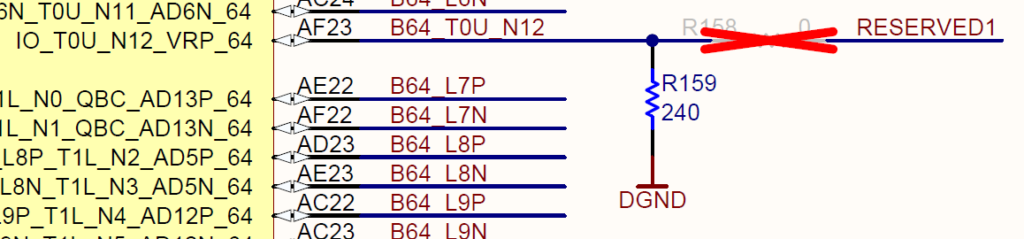
Please see the UltraScale Architecture SelectIO Resources for more details about the VRP pin and IOSTANDARD support.
Considerations for Differential Signals
The XEM8305 PCB layout and routing has been designed with several applications in mind, including applications requiring the use of differential (LVDS) pairs. Please refer to the Artix UltraScale+ datasheet for details on using differential I/O standards with the Artix UltraScale+ FPGA.
FPGA Differential I/O Standards
The different I/O banks on the Artix UltraScale+ have different features and specific requirements needed to use differential I/O standards.
HP banks support LVDS inputs and outputs. The bank VCCO must be set to 1.8V to use LVDS outputs. This also allows the use of the available internal termination on LVDS inputs.
HD banks only support LVDS inputs, and only with external termination. The XEM8305 provides optional external termination resistor positions under the FPGA. As such termination would interfere with the I/O being used as single ended connections, these termination resistors are not populated by default. See the table below to find the termination resistor designator for each HD bank differential pair. The resistor designators are marked on the PCB silkscreen. 100 Ohm resistors can be placed as external termination for each pair.
Please see LVDS Interface Checklist for more information. Also see DS931 for information regarding the LVDS DC Specifications on the Artix UltraScale+. For more information on the differential I/O standard limitations of HD banks see the “High Density I/O Resources” section of UG571.
HD Bank Optional External Differential Termination Designators
| Diff Pair | Termination Designator | Diff Pair | Termination Designator |
|---|---|---|---|
| B85_L1 | R73 | B84_L7 | R93 |
| B85_L2 | R74 | B84_L8 | R94 |
| B85_L3 | R75 | B84_L9 | R95 |
| B85_L4 | R76 | B84_L10 | R96 |
| B85_L5 | R77 | B84_L11 | R97 |
| B85_L6 | R78 | B84_L12 | R100 |
| B85_L7 | R79 | B86_L1 | R102 |
| B85_L8 | R80 | B86_L2 | R160 |
| B85_L9 | R81 | B86_L3 | R161 |
| B85_L10 | R82 | B86_L4 | R162 |
| B85_L11 | R83 | B86_L5 | R163 |
| B85_L12 | R84 | B86_L6 | R165 |
| B84_L1 | R85 | B86_L7 | R166 |
| B84_L2 | R86 | B86_L8 | R167 |
| B84_L3 | R87 | B86_L9 | R169 |
| B84_L4 | R88 | B86_L10 | R170 |
| B84_L5 | R91 | B86_L11 | R171 |
| B84_L6 | R92 | B86_L12 | R172 |
Characteristic Impedance
Single-ended fabric I/O are routed to the expansion connectors with 50Ω characteristic impedance. Differential fabric I/O and transceiver signals are routed to the expansion connectors as pairs with 100Ω differential impedance.
Differential Pair Lengths
It is desirable that the route lengths of a differential pair be matched within some specification. Care has been taken to route differential pairs on the FPGA to adjacent pins on the expansion connectors, and the length of all pairs is matched to within 5 mils (including pin/package delays). Individual PCB routing lengths for all expansion connections are available on the XEM8305 Pins Reference page. The lengths published there represent routed PCB lengths only and do not include the pin/package delays. Pin/package delay information may be obtained from the AMD design tools.
Length Matching to Carriers
Trace length matching to control signal propagation delay is often an important factor in PCB design. Opal Kelly FPGA modules have varying I/O trace lengths from the FPGA to the expansion connectors, as required by the space constraints of each module PCB. These PCB trace lengths are published on our Pins site for each specific board.
Details on using the Pins data to length match the entire signal from FPGA to carrier hardware can be found on our Length Matching Carrier Boards page.
I/O State at Power On
Artix UltraScale+ FPGAs support a weak pull-up state on all I/O pins from power on until first configuration. This behavior is controlled by the PUDC_B pin. By default the XEM8305 holds the PUDC_B pin high with a 1kΩ resistor at R125, disabling the weak pull-up on all I/O pins at power on. This behavior can be changed by inserting a 1kΩ resistor at R128 and removing the 1kΩ resistor at R125, pulling the PUDC_B pin to ground.