Powering the ZEM5310
The ZEM5310 requires a clean, filtered, DC supply within the range of 4.5 V to 5.5 V. This supply must be delivered through the DC power connector or from the corresponding pins on MC1.
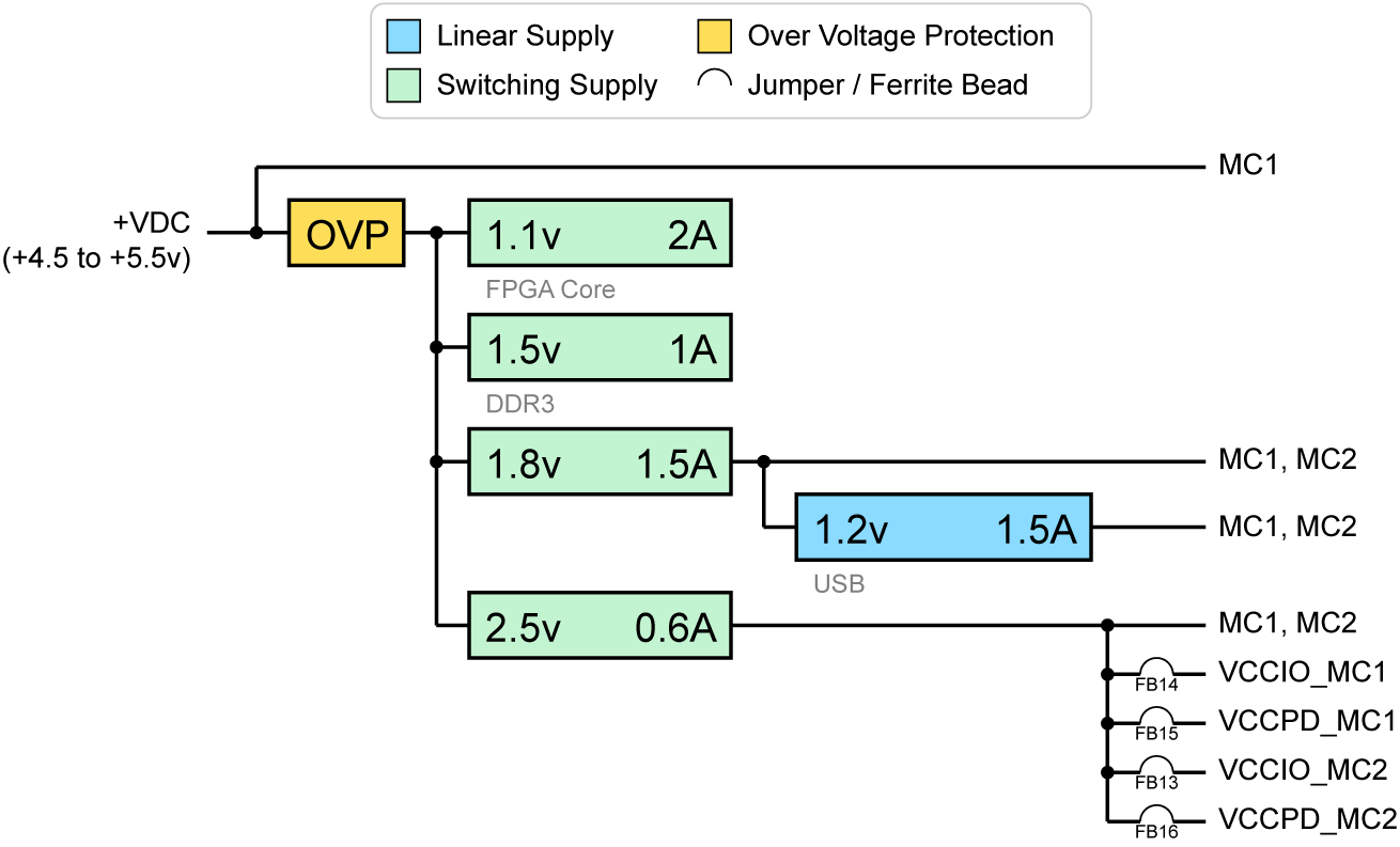
The ZEM5310 power distribution system is rather complex, with several supplies designed to provide suitable, efficient power for several systems and modules. A schematic diagram of the system follows, with input (+VDC) shown to the left and accessible supply rails shown to the right.
Power Supply
The ZEM5310 is designed to be operated from a single 5-volt power source supplied through the DC power jack on the device. This provides power for the several high-efficiency switching regulators on-board to provide multiple DC voltages for various components on the device.
DC Power Connector
The DC power connector on the ZEM5310 is part number PJ-102AH from CUI, Inc. It is a standard “canon-style” 2.1mm / 5.5mm jack. The outer ring is connected to DGND. The center pin is connected to +VDC.
Powering via USB
The ZEM5310 has been designed to accept power (+5VDC only) via the USB connector with a small modification. To power from USB, you will need to install a 0 Ω resistor (0603 dimension) at location R48, located on the reverse side of the PCB under the power connector. This will connect the +5VUSB from the USB connector to the +5VDC on the ZEM5310.
With this resistor in place, you should not apply +5VDC to the external power connector.
I/O Triples
For each Altera FPGA I/O bank, there are three relevant power supplies. We call these three supplies an I/O Triple. These triples are set according to the I/O standard(s) required for I/O on the bank. Please refer to the extensive Altera documentation for more information on which settings are required for each standard.
- VCCIO – The I/O supply and is set according to the I/O standard selected for the bank.
- VCCPD – The pre-driver voltage for the bank. It is set according to:
- If VCCIO = 3.3v, set VCCPD = 3.3v
- If VCCIO = 3.0v, set VCCPD = 3.0v
- If VCCIO ≤ 2.5v, set VCCPD = 2.5v
- VREF – This is a reference voltage required for some standards. Note that this is not required for many of the supported I/O standards.
| FPGA BANK | FPGA SUPPLY | EXPANSION PINS | RESTRICTIONS |
|---|---|---|---|
| 2, 5 | VCCIO_MC1 | MC1-36 MC1-56 |
None See Altera documentation for details. |
| VCCPD_MC1 | MC1-12 | ||
| VREF_MC1 | MC1-10 | ||
| 3, 4 | VCCIO_MC2 | MC2-35 MC2-55 |
None Note that VCCPD_MC2 also provides VCCPD to the USB host interface banks. When running at a non-default supply voltage please update the pin constraints for the host interface pins (okUH, okHU, and okUHU) to match the supplied VCCPD voltage. |
| VCCPD_MC2 | MC2-12 | ||
| VREF_MC2 | MC2-10 |
Power Budget
The table below can help you determine your power budget for each supply rail on the ZEM5310. All values are highly dependent on the application, speed, usage, and so on. Entries we have made are based on typical values presented in component datasheets or approximations based on Altera power estimator results. Shaded boxes represent unconnected rails to a particular component. Empty boxes represent data that the user must provide based on power estimates.
The user may also need to adjust parameters we have already estimated (such as FPGA Vcco values) where appropriate. All values are shown in milliwatts (mW).
Notes:
- Per the diagram above, the 1.2v supply is downstream of the 1.8v supply, so available power should be considered.
- The 1.2v supply is subject to up to 800 mA of inrush during the power sequencing.
| COMPONENT(S) | 1.1V | 1.2V | 1.5V | 1.8V | 2.5V |
|---|---|---|---|---|---|
| 100 MHz | 80 | ||||
| USB, DDR3, Flash | 320 | 410 | 40 | 250 | |
| FPGA | 350 | 725 | |||
| FPGA Core | |||||
| FPGA Vcco | |||||
| Total (mW) | |||||
| Available (mW) | 2,200 | 1,800 | 1,500 | 2,700 | 1,500 |
Example ZEM5310-A4 FPGA Power Consumption
Altera PowerPlay Power Estimator version 15.0 was used to compute the following power estimates for the Vccint supply. These are simply estimates; your design requirements may vary considerably. The numbers below indicate approximately 80% utilization.
| COMPONENT | PARAMETERS | VCCINT |
|---|---|---|
| Clock | 200 MHz CLK, 60,000 fanout | 239 mW |
| Logic (DFF) | 50% 100 / 50% 200 MHz, 60,000 DFFs 50% 100 / 50% 200 MHz, 24,000 LUTs | 347 mW |
| RAM | 120 single-port M10K at 100 MHz 120 dual-port M10K at 200 MHz 100 dual-port MLAB at 200 MHz | 149 mW |
| DSP | 110 DSPs at 200 MHz | 101 mW |
| Memory Controller | 400 MHz, DDR3 | 140 mW |
| Misc. | DCM, PLL, etc. | 35 mW |
| Total | 1,011 mW | |
| Available | 2,000 mW |