Powering the XEM8305
The XEM8305 requires a clean, filtered, DC supply within the range of 5V to 15V. The recommended supply voltage is 12V. This supply must be delivered through the expansion connector (rated to 4A max current).
Power Supply
The XEM8305 is designed to be operated from a single power supply of 5V to 15V supplied through the expansion connector on the device. This provides power for the several high-efficiency switching regulators on-board to provide multiple DC voltages for various components on the device as well as three adjustable supplies for the peripheral.
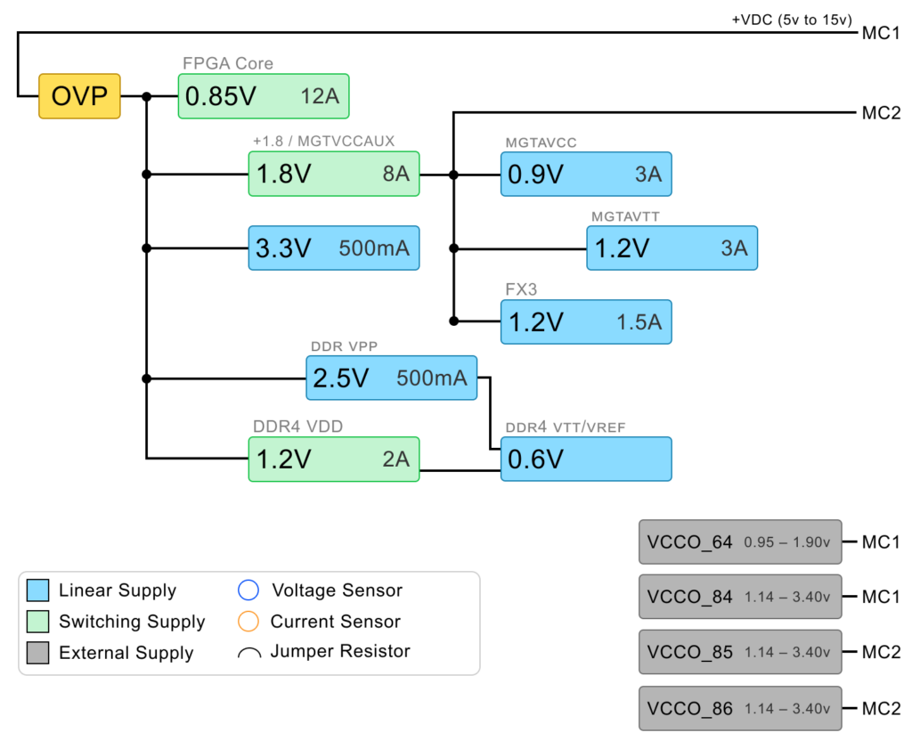
A block diagram of the power distribution system is shown below.
Expansion Connector Power
Power for the XEM8305 is connected through the expansion connector MC1. A supply voltage from 5V to 15V must be provided. The suggested nominal supply voltage is 12V. The power input on the expansion connector is rated for up to 4A.
Find the pin connections in the Pins sheet.
Input Power Protections
The XEM8305 includes an over-voltage protection circuit which disconnects the input supply from the on-board circuitry when the input is higher than 15V (28 V absolute maximum). It is also prevented from powering on when the input supply is below 4.5V. The input current is limited to 5A, and it is protected from a reverse polarity voltage connection.
External I/O Voltage
The XEM8305 requires external power input for the VCCO I/O rails. The VCCO I/O rails are connected directly to the expansion connector without any onboard regulators. Power must be supplied through the expansion connectors at the desired I/O voltage.
The VCCO I/O rails should be powered only after the rest of the FPGA power rails are up and good. The XEM8305_PG signal available on MC1 can be used to sequence the power on of external VCCO I/O regulators. FPGA power is good when this signal is high with a 1.8V signal level.
The XEM8305 provides a 1.8V power output on the expansion connector MC2. This voltage falls in the valid range for all VCCO I/O rails and can be used to power the rails if externally connected to the VCCO I/O expansion connector pins on the carrier board. This rail already provides the correct power sequencing for the VCCO I/O inputs.
Find the pin connections in the Pins sheet.
| VCCO Rail | Bank Type | Voltage Range |
|---|---|---|
| VCCO_64 | HP | 0.95v – 1.90v |
| VCCO_84 | HD | 1.14v – 3.40v |
| VCCO_85 | HD | 1.14v – 3.40v |
| VCCO_86 | HD | 1.14v – 3.40v |
LED Indicators
The XEM8305 includes three LED indicators for power status.
| LED | ON CONDITION |
|---|---|
| PWR IN (D8) | +VDCIN present and valid |
| PWR GOOD (D9) | All on-board power supplies active and within expected range (Does not include external VCCO rails) |
| FAULT (D11) | Indicates an invalid input voltage or overcurrent. |
Power Budget
The table below can help you determine your power budget for each supply rail on the XEM8305. All values are highly dependent on the application, speed, usage, and so on. Entries we have made are based on typical values presented in component datasheets or approximations based on AMD power estimator results. Empty boxes represent data that the user must provide based on power estimates.
The user may also need to adjust parameters we have already estimated where appropriate. All values are shown in milliwatts (mW) unless otherwise specified.
| COMPONENT(S) | 0.85 V | 1.2 V | 1.8 V | 2.5 V |
|---|---|---|---|---|
| FPGA VCCINT, VCCINT_IO, VCCBRAM | — | — | — | |
| FPGA VCCAUX, VCCAUX_IO, VCCADC | — | — | 1,031 | — |
| Clock oscillators | — | — | 120 | — |
| FPGA MGTYAVCC | — | — | 2228 | — |
| FPGA MGTYAVTT | — | — | 4444 | — |
| FPGA MGTYVCCAUX | — | — | 241 | — |
| FX3 USB host interface | — | — | 648 | — |
| DDR4 VDD/VDDQ | — | 396 | — | — |
| DDR4 VTT termination | — | 231 | — | — |
| DDR4 VPP | — | — | — | 71 |
| FPGA VCCO | — | 158 | — | |
| Total (mW) | 1441 | 8,712 | 71 | |
| Available (mW) | 10,200 | N/A | 10,800 | N/A |
Example FPGA Power Consumption
AMD Power Estimator (XPE) version 2022.2.1 was used to compute the following power estimates for the VCCINT supply. These are simply estimates; your design requirements may vary considerably. The numbers below indicate approximately 80% utilization.
| COMPONENT | PARAMETERS | VCCINT POWER (MW) |
|---|---|---|
| Clock | 400 MHz GCLK, 124,560 fanout | 627 |
| Clock | 500 MHz GCLK, 15,977 fanout | 302 |
| Clock | 500 MHz (PCIe Gen4) GCLK, 7,208 fanout | 142 |
| Logic | 400 MHz, 62,400 logic LUTs, 124,000 registers | 1,848 |
| Logic | 500 MHz, 8,045 logic LUTs, 15,977 registers | 298 |
| Logic | 500 MHz (PCIe Gen4), 3,354 logic LUTs, 7,208 registers | 129 |
| BRAM | 36-bit, 500 MHz, 80 block RAMs, 12.5% toggle rate | 177 |
| BRAM | 36-bit (PCIe Gen4), 500 MHz, 22 block RAMs, 12.5% toggle rate | 45 |
| DSP | 600 MHz, 460 slices, 12.5% toggle rate | 1,132 |
| GTH | 12 channels, 16 Gb/s | 1242 |
| Misc. | DCM, PLL, VCCINT_IO, etc. | 100 |
| Total | 5,942 mW | |
| Available | 10,200 mW |