BRK8305 Breakout Board
Unlike our integration modules, breakout boards are not intended for production integration. We reserve the right to change dimensions and functionality of this board at any time and may not necessarily have the previous version available for purchase.
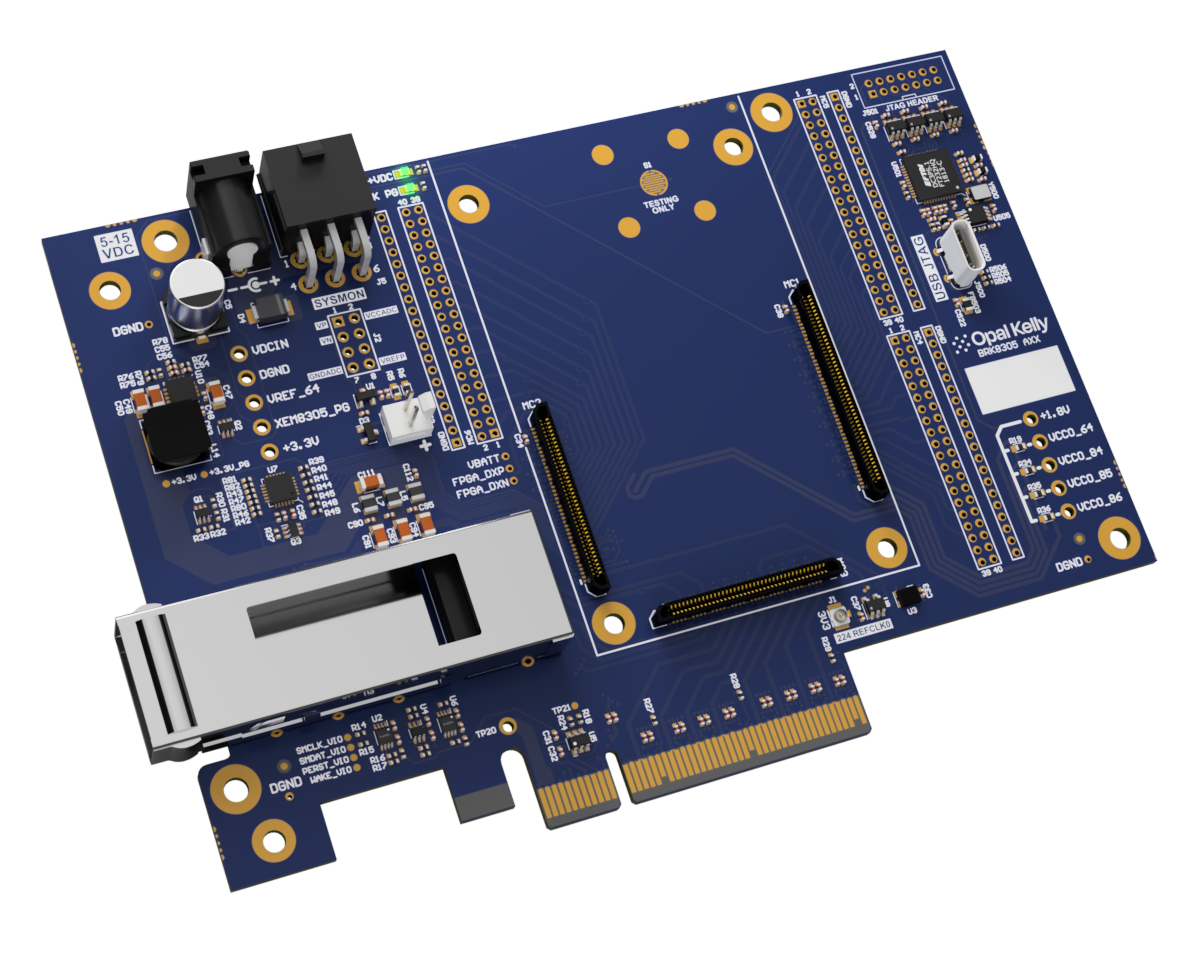
Peripherals and Connectors
The table below summarizes the various connectors on the BRK8305. The XEM8305 Pin List has connection information in the BRK8305 column. Additionally, please refer to the schematics and layout available on the Downloads section of the Pins website for detailed connection diagrams.
| CONNECTOR TYPE | REFDES | FPGA CONNECTION | |
|---|---|---|---|
| PCIE | J6 | GTY224, GTY225 | TxRx 0-3 |
| QSFP | J30 | GTY226 | TxRx 0-3 |
| 2mm Header | MC4 | Bank 64, 84 | 36 I/O |
| 2mm Header | MC5 | Bank 64 | 40* I/O |
| 2mm Header | MC6 | Bank 85, 86 | 37 I/O |
| JTAG Header | J3 | JTAG Pins |
* 1 of the MC5 I/O pins is normally used on the XEM8305 for a VRP resistor and not available as I/O without moving a resistor on the XEM8305
Power Connectors
The BRK8305 has a barrel jack power connector (J4) and a 6-pin PCIe connector (J5) that accept 5V to 15V, 12V nominal. This input voltage is passed to the XEM8305’s expansion connector.
Barrel Jack Power Connector
The barrel jack power connector on the BRK8305 is part number PJ-102AH from CUI, Inc. It is a standard “canon-style” 2.1mm / 5.5mm jack. The outer ring is connected to DGND, the center pin is +VDCIN. The PJ-102AH jack is rated for 5 A maximum continuous current.
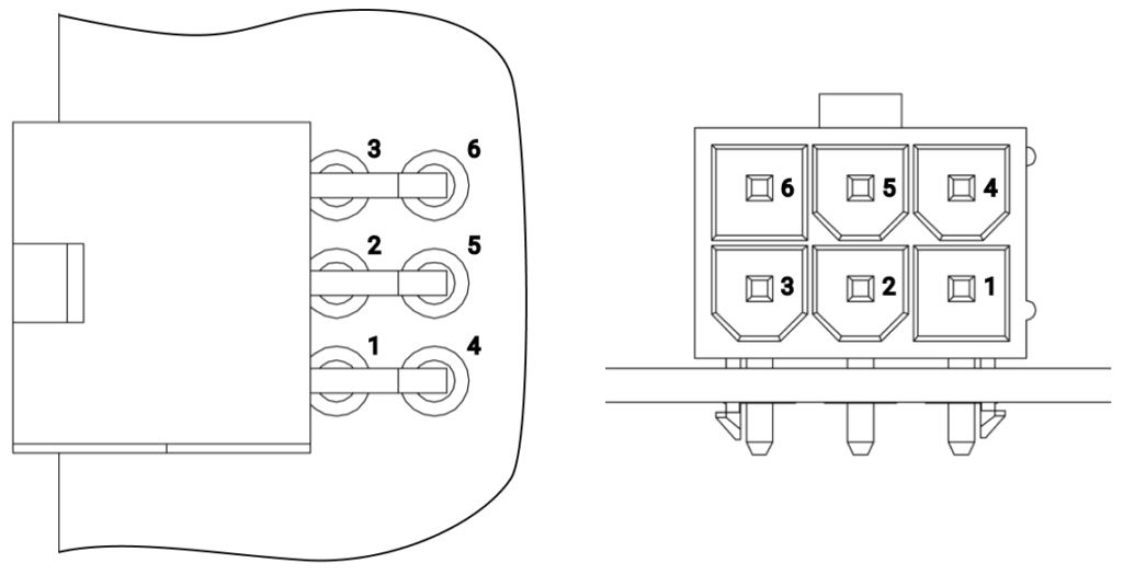
6-Pin Power Connector
The 6-pin connector is a PCIe-style power connector from Molex, part number 0455580003. Pins 1-3 are connected to +VDCIN, and pins 4-6 are connected to DGND. Maximum current is 24 A (8 A per pin).
JTAG
The BRK8305 has a built in USB JTAG adapter. Connect to the USB-C connector J500 for AMD tools compatible access to the XEM8305’s JTAG interface.
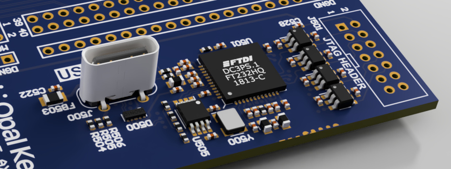
The JTAG connections are also wired to a dedicated 2mm header J501 that can be used with a compatible JTAG cable. The JTAG interface presented is at a 1.8V signaling voltage. This header is not populated by default. This footprint is compatible with the Molex part 87831-1420.
| CONNECTOR PIN | JTAG SIGNAL | CONNECTOR PIN | JTAG SIGNAL |
|---|---|---|---|
| 1 | GND | 2 | +1.8V (Vref) |
| 3 | GND | 4 | JTAG_TMS |
| 5 | GND | 6 | JTAG_TCK |
| 7 | GND | 8 | JTAG_TDO |
| 9 | GND | 10 | JTAG_TDI |
| 11 | GND | 12 | NC |
| 13 | GND | 14 | NC |
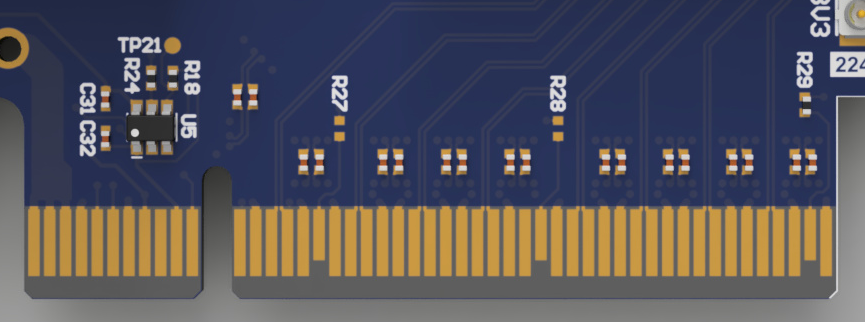
PCIE Connector Fin
The BRK8305 is designed to slot into a standard computer PCIE x8 and larger connector. This allows for a high bandwidth PCIE host connection.
PCIE Lanes
The BRK8305 supports up to a x8 PCIE connection and is configured for x8 lanes by default. This is the maximum PCIE width supported by Artix UltraScale+. For more information see the PG213 section ‘Artix UltraScale+ Devices Available GT Quads’.
A x1 or x4 lane connection can be configured if required. To change the configured number of lanes, place the PCIE_PRSNT jumper resistor in the appropriate location as defined in the table on the BRK8305 schematic.
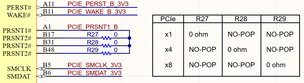
Control Signals
Voltage level shifting of PERST, WAKE and SMBus signals to the host is handled on the BRK8305 to change the signals from the I/O voltage level to 3.3V used by the PCIE fin. Control IO signals across the connector are disabled if either side is unpowered.
| Signal | Expansion Connector Pin | FPGA Pin | VCCO |
|---|---|---|---|
| PERST | MC2 – 15 | J11 | VCCO_85 |
| WAKE | MC2 – 17 | J10 | VCCO_85 |
| SDA (SMBus) | MC2 – 13 | K9 | VCCO_85 |
| SCL (SMBus) | MC2 – 11 | K10 | VCCO_85 |
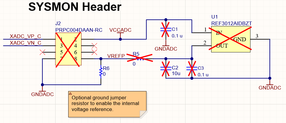
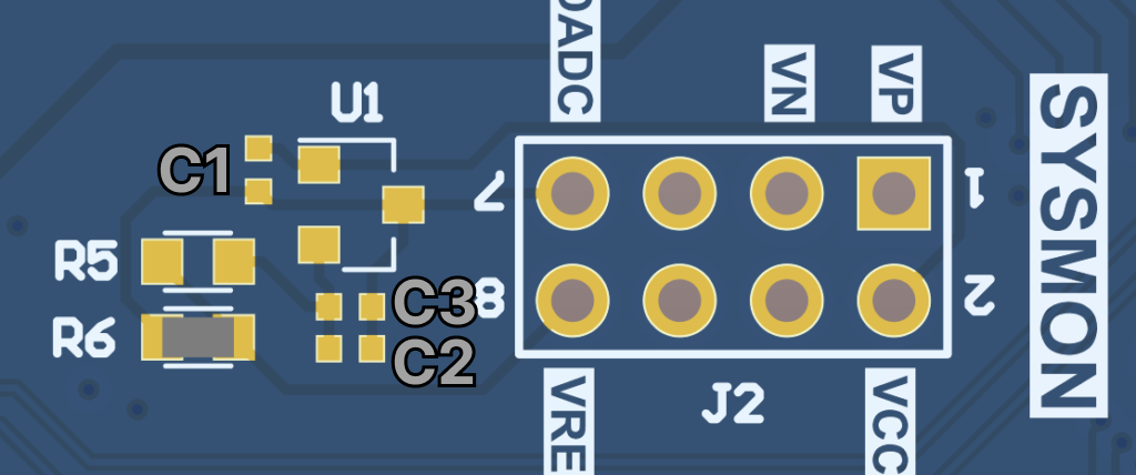
ADC Voltage Reference
By default BRK8305 includes a 0R jumper that enables the XEM8305 FPGA’s internal ADC voltage reference. However part footprints are included for adding an external high precision reference voltage IC if required.
To use the external 1.25V voltage reference part REF3012AIDBZT or compatible:
- Remove jumper resistor
R6 - Place voltage reference
U1 - Place capacitors
C1,C2andC3 - Place jumper resistor
R5
QSFP+
A QSFP+ port is connected to the XEM8305’s quad 226 transceiver to allow for easy connection of QSFP+ modules. Full QSFP+ transceiver connection pinout and control signal I/O connections are listed on the XEM8305 Pin List.
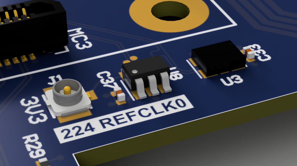
Refclk
To facilitated common QSFP+ protocols a 156.25Mhz oscillator is included on the BRK8305 and connected to the XEM8305’s quad 226 refclk 0 input.
| Signal | EXPANSION CONNECTOR PIN | FPGA PIN |
|---|---|---|
| MGT_REFCLK0P_226_C | MC2 – 2 | P7 |
| MGT_REFCLK0N_226_C | MC2 – 4 | P6 |
Control Signals
Voltage level shifting of the QSFP+ signals to the host is handled on the BRK8305 to change the signals from the I/O voltage level to 3.3V used by the QSFP+ module. Control IO signals across the connector are disabled if either side is unpowered.
| SIGNAL | EXPANSION CONNECTOR PIN | FPGA PIN | VCCO |
|---|---|---|---|
| INT_B | MC2 – 19 | J9 | VCCO_85 |
| MODPRS_B | MC2 – 21 | H9 | VCCO_85 |
| RESET_B | MC2 – 23 | H11 | VCCO_85 |
| MODSEL_B | MC2 – 25 | G11 | VCCO_85 |
| LP_MODE | MC2 – 27 | G10 | VCCO_85 |
| SDA | MC2 – 29 | G9 | VCCO_85 |
| SCL | MC2 – 31 | F10 | VCCO_85 |
Clock Oscillators
The XEM8305 provides three MGT refclock inputs on its expansion connectors. This table lists the refclock connections on the BRK8305.
| REFCLOCK | FPGA PIN | Freqency | Designator |
|---|---|---|---|
| REFCLK0P 224 / REFCLK0N 224 | AB7 / AB6 | User Input SE Clock | J1 |
| REFCLK0P 225 / REFCLK0N 225 | V7 / V6 | PCIE Host Refclock | J6 |
| REFCLK0P 226 / REFCLK0N 226 | P7 / P6 | 156.25Mhz | U3 |
The Quad 224 refclock0 input uses a single ended to LVDS converter onboard the BRK8305. A 3.3V single ended clock of the desired frequency can be connected to the U.FL connector J1, and it will be converted to an LVDS refclock input.
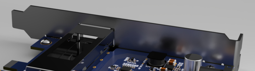
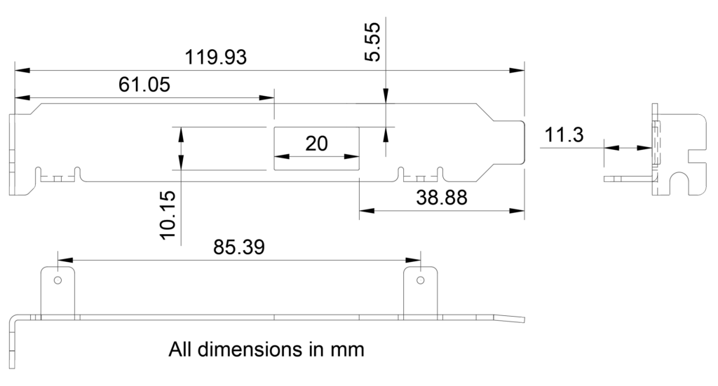
PCIE Bracket
The BRK8305 is designed to slot into a standard x8 or larger PCIE slot. It has mounting holes to attach a PCIE bracket for mechanical support. The PCIE bracket requires a cutout for the QSFP port. A mechanical drawing is provided below. Attaching the bracket to the BRK8305 requires two 5/32″ long 4-40 machine screws.
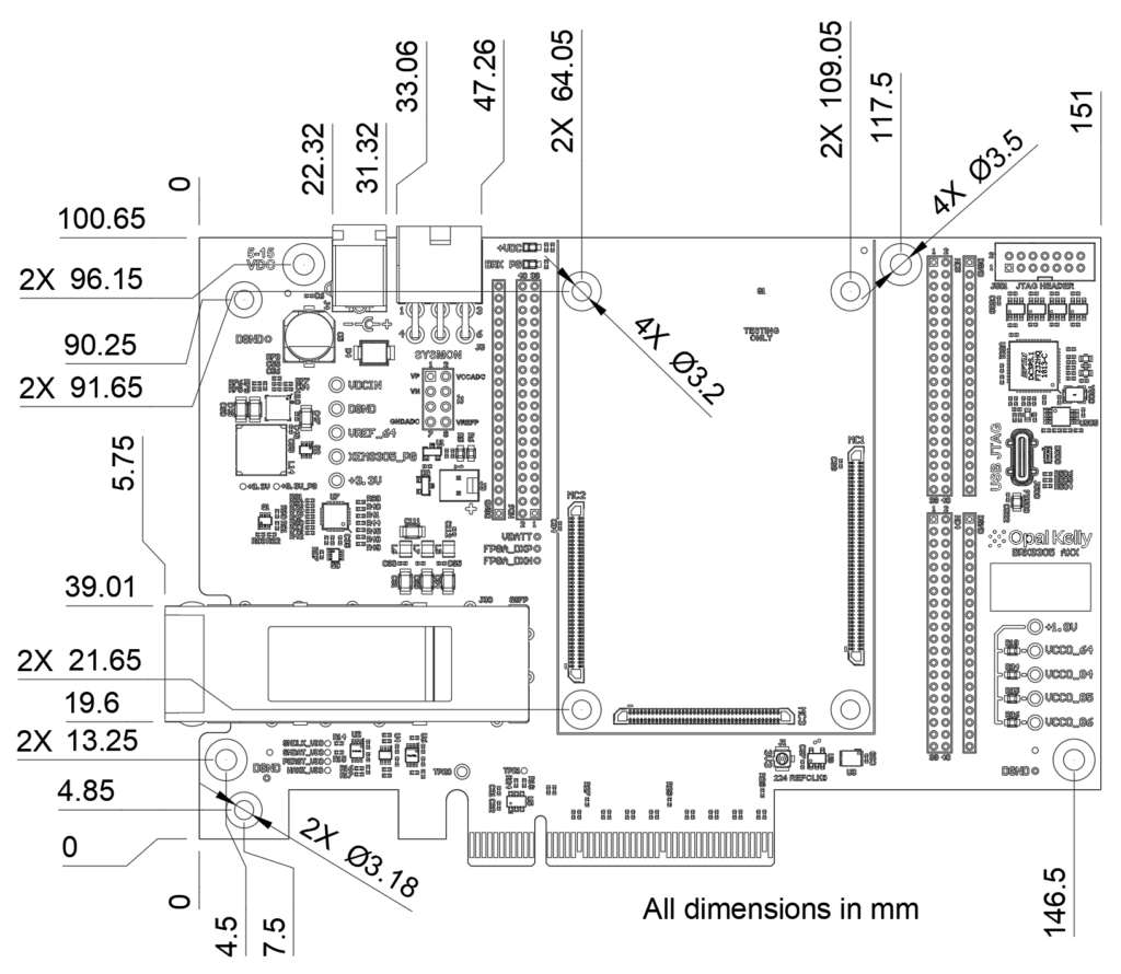
Mechanical Drawing
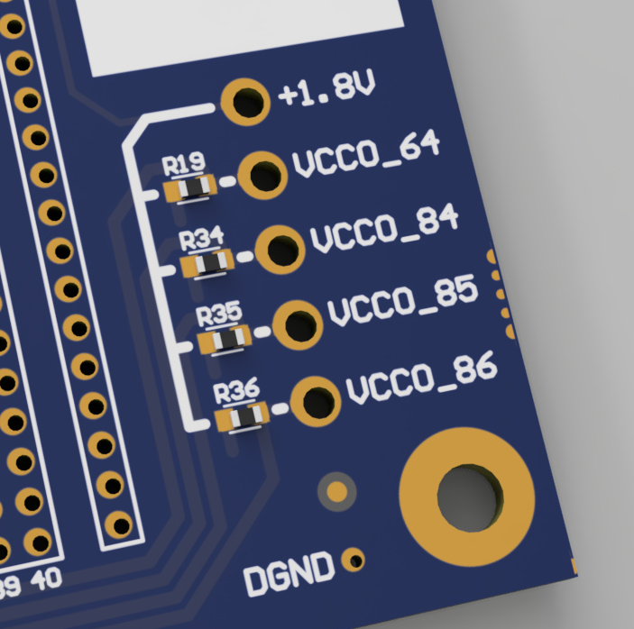
I/O Voltage
The XEM8305 requires externally supplied voltage for it’s I/O banks. By default 0 Ohm jumper resistors are placed on the BRK8305 to connect the XEM8305’s provided 1.8V rail to each of the I/O banks. To use any other voltage for an I/O bank, the jumper resistor must be removed, and the external voltage connected to the I/O banks VCCO test point
More information on supplying external bank I/O power can be found on the Powering the XEM8305 page.
| I/O Bank Power | Jumper Resistor Designator |
|---|---|
| VCCO 64 | R19 |
| VCCO 84 | R34 |
| VCCO 85 | R35 |
| VCCO 86 | R36 |
Impedance and Length Matching
Single-ended fabric I/O are routed to the breakout connectors with 50Ω characteristic impedance. Differential fabric I/O and transceiver signals are routed to the breakout connectors as pairs with 100Ω differential impedance.
Schematic and Design Files
The BRK8305 schematics and design files are available in the Downloads section of the Pins website.
Mechanical Drawing
The mechanical drawing below may be used for enclosure or mounting hardware design. 3D Models are also available in SolidWorks, STEP, and IGES formats.