Powering the XEM8310
The XEM8310 requires a clean, filtered, DC supply within the range of 7.5 V to 15 V. This supply may be delivered through the barrel jack power connector (rated to 5 A max current) or through the mezzanine connector (rated to 8 A max current).
Power Supply
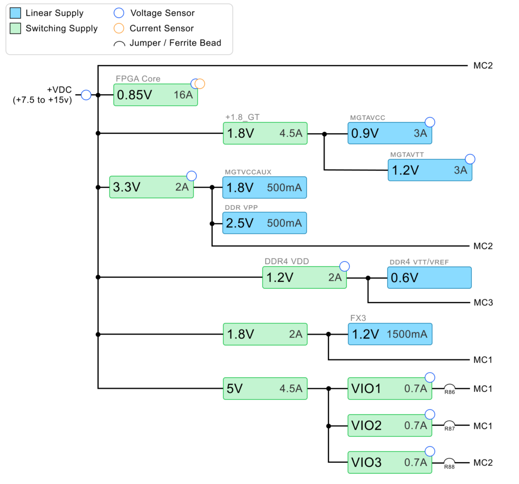
The XEM8310 is designed to be operated from a single power supply of 7.5 V to 15 V supplied through the DC power jack on the device. This provides power for the several high-efficiency switching regulators on-board to provide multiple DC voltages for various components on the device as well as three adjustable supplies for the peripheral.
A block diagram of the power distribution system is shown below.
The optional fansink for the XEM8310 has an operating range of 10.8 V to 13.2 V, with a nominal operating voltage of 12 V. It is recommended to keep the external supply voltage within this range whenever the fansink is enabled.
Barrel Jack Power Connector
The barrel jack power connector on the XEM8310 is part number PJ-102AH from CUI, Inc. It is a standard “canon-style” 2.1mm / 5.5mm jack. The outer ring is connected to DGND. The center pin is connected to +VDCIN.
The PJ-102AH jack is rated for 5 A maximum continuous current. Applications requiring higher current must use the mezzanine connectors for providing power to the system (rated for a maximum of 8 A).
LED Indicators
The XEM8310 includes two LED indicators for power status.
| LED | On Condition |
|---|---|
| PWR IN (D5) | +VDCIN present (>2V) |
| PWR GOOD (D6) | All on-board power supplies active and within expected range (Does not include VIOx supplies) |
Power Budget
The table below can help you determine your power budget for each supply rail on the XEM8310. All values are highly dependent on the application, speed, usage, and so on. Entries we have made are based on typical values presented in component datasheets or approximations based on AMD power estimator results. Shaded boxes represent unconnected rails to a particular component. Empty boxes represent data that the user must provide based on power estimates.
The user may also need to adjust parameters we have already estimated (such as FPGA VCCO values) where appropriate. All values are shown in milliwatts (mW) unless otherwise specified.
| COMPONENT(S) | 0.85 V | 1.2 V | 1.8 V | 1.8 V GT | 3.3 V |
|---|---|---|---|---|---|
| FPGA VCCINT, VCCINT_IO, VCCBRAM | |||||
| FPGA VCCAUX, VCCAUX_IO, VCCADC | 956 | ||||
| Clock oscillators | 165 | ||||
| FPGA MGTYAVCC | 2228 | ||||
| FPGA MGTYAVTT | 4444 | ||||
| FPGA MGTYVCCAUX | 241 | ||||
| FX3 USB host interface | 648 | ||||
| DDR4 VDD/VDDQ | 792 | ||||
| DDR4 VTT termination | 461 | ||||
| DDR4 VPP | 142 | ||||
| FPGA VCCO | 188 | 297 | |||
| Total (mW) | 1441 | 1901 | 6673 | 548 | |
| Available (mW) | 13,600 | 2,400 | 3,600 | 8100 | 6,600 |
| COMPONENT(S) | VIO1 | VIO2 | VIO3 |
|---|---|---|---|
| FPGA VCCO | |||
| SYZYGY Group 1 | |||
| SYZYGY Group 2 | |||
| SYZYGY Group 3 | |||
| Total (mW) | |||
| Available (mW) | 700 mA 1.0-1.8 V | 700 mA 1.2-3.3 V | 700 mA 1.2-3.3 V |
Example FPGA Power Consumption
AMD Power Estimator (XPE) version 2020.2.2_1 was used to compute the following power estimates for the VCCINT supply. These are simply estimates; your design requirements may vary considerably. The numbers below indicate approximately 80% utilization.
| COMPONENT | PARAMETERS | VCCINT POWER (mW) |
|---|---|---|
| Clock | 200 MHz GCLK, 200,000 fanout | 986 |
| Clock | 300 MHz GCLK, 75,000 fanout | 628 |
| Clock | 100 MHz GCLK, 100,000 fanout | 272 |
| Clock | 667 MHz GCLK, 50,000 fanout | 963 |
| Logic | 200 MHz, 58,000 logic LUTs, 20,000 shift registers, 20,000 distributed RAMs, 150,000 registers | 1,566 |
| Logic | 300 MHz, 8,000 logic LUTs, 75,000 registers | 583 |
| Logic | 667 MHz (DDR4), 16,000 logic LUTs, 50,000 registers | 1,149 |
| BRAM | 18-bit, 200 MHz, 280 block RAMs, 50% toggle rate | 519 |
| BRAM | 36-bit, 300 MHz, 140 block RAMs, 50% toggle rate | 920 |
| DSP | 300 MHz, 1090 slices, 12.5% toggle rate | 1,503 |
| GTY | 11 channels, 16.3 Gb/s | 727 |
| Misc. | DCM, PLL, VCCINT_IO, etc. | 100 |
| Total | 9,916 mW | |
| Available | 13,600 mW |