Length Matching Carrier Boards
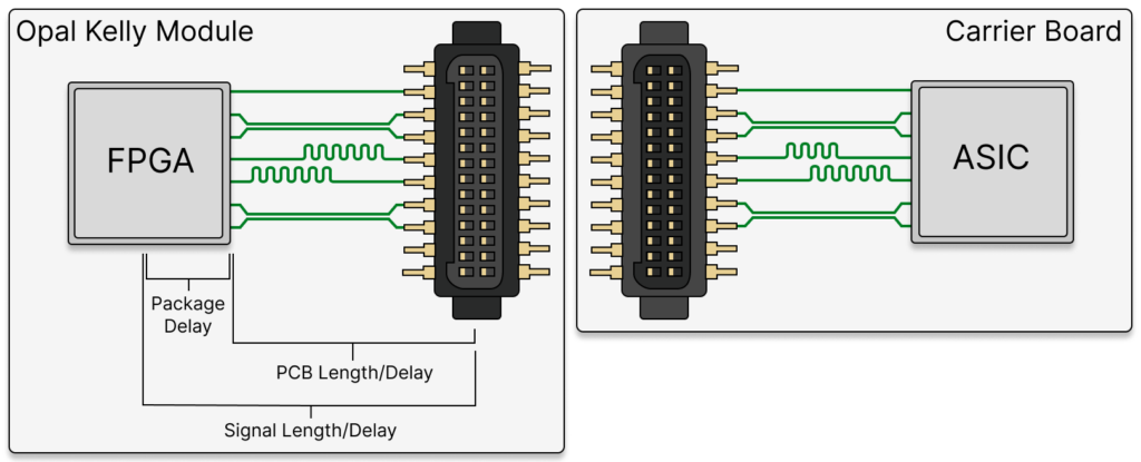
Trace length matching to control signal propagation delay is often an important factor in PCB design. Opal Kelly FPGA modules have varying I/O trace lengths from the FPGA to the expansion connectors, as required by the space constraints of each module PCB. These PCB trace lengths are published on our Pins site for each specific board.
Customer designed carrier boards may need to take these trace lengths into account depending on their specific requirements. There are various methods to import the module trace length data into a carrier design depending on the PCB tools used.
Pins Spreadsheet PCB Length/PCB Delay Details
Our Pins spreadsheets list the PCB trace length between the FPGA and the expansion connector. However, this doesn’t represent the entire signal delay. There are additional delays from the pin package connections internal to the FPGA. These delays are published by the FPGA manufacture. To include the total signal delay in your carrier board design you must sum both of these delays. Use the instructions below to generate the total I/O signal length/delay for each expansion connector pin.
These signal delays can be used in your carrier design to length match the entire signal path from the FPGA to your onboard hardware. The delay values can be added to the carrier side expansion connector pins delay parameters to let your PCB software include them in the total route delay during length matching. Instructions for including these signal delays in an Altium design are included below.
Prepare Module I/O Signal Data Delay
- Export the Pins spreadsheet for the FPGA module as a CSV file.
- Open the exported Pins spreadsheet.
- Make sure the sheet is sorted first by the expansion connector designator, and then the expansion connector pin number.
- If the
Package Delay (ps)is not already included in the Pins sheet, it will need to be acquired from the FPGA manufacture and added as a column to the table. - Create a new column next to the
PCB Length (mm)column titledSignal Length (mm) - Use an expression to fill this column:
- The
PCB Length (mm)Value + (ThePackage Delay (ps)value * 0.15) - 0.15 is a constant used to estimate the pin package length from the picosecond delay value based on an assumed signal propagation speed in the FPGA package.
- The
- If the Pins list contains a
PCB Delay (ps)column, create a new column next to it titledSignal Delay (ps) - Use an expression to fill this column:
- The
PCB Delay (ps)value + ThePackage Delay (ps)value
- The
Altium Batch Pin/Package Assignment
Use these instructions to add the FPGA module signal delay values to the pin package delays of the expansion connector parts on a carrier board. This way they will be included in the total signal routing computations while length matching.
Length values copied into the Altium schematic pin package values need to be in mils, and the Pins table data is in mm. Add a new column titled Signal Length (mil) to convert the mm values to mils by multiplying the mm value by 39.37, and use those values to copy into the Altium schematic pins.
- Use the Pins spreadsheet generated above. Make sure to use the
Signal Length (mil)values in mils, and not the mm values. - Open the Altium schematic page for your carrier board with the expansion connectors on it.
- Create a
SCH Filter(View -> Panels -> SCH Filter) with the following search query. Make sure the “Select” option of the schematic filter is checked. Substitute'MC1'with your expansion connector designator.(ObjectKind = 'Pin') and (OwnerName = 'MC1')
- Apply the filter to select all of the pins of the expansion connector.
- In the
SCH Listview (View -> Panels -> SCH List), sort the table byPin Designatorin order to sort the pins by expansion connector pin number (this order must match the Pins spreadsheet order). - Scroll to find the
Pin/Pkg LengthandPropagation Delaycolumns. - In the Pins spreadsheet select the data from the
Signal Length (mil)orSignal Delaycolumn (see creation of columns above), starting from the current expansion connector pin 1 to the last pin for that expansion connector, and copy the data to the clipboard (Include any blank cells). - In the
SCH Listview, select the entire column forPin/Pkg LengthorPropagation Delay(depending on which data you just copied from the Pins spreadsheet) by clicking on the first cell, and then shift+clicking on the last cell.- Note: Some expansion connectors have a Pin 0 ground connection. In this case skip the first row (pin 0) in your selection).
- Paste in the pin package values copied from the Pins spreadsheet (from the clipboard).
- Repeat copying the data for the
Signal Length (mil)orSignal Delaycolumn as necessary (Steps 7 to 9). - Repeat steps 3 to 10 for each expansion connector on your carrier board.
- Update the PCB with the new expansion connector pin package values that were added to the schematics.